ZHCSG94L August 2013 – February 2019 TPS659038-Q1 , TPS659039-Q1
PRODUCTION DATA.
- 1 器件概要
- 2 修订历史记录
- 3 Device Comparison
- 4 Pin Configuration and Functions
-
5 Specifications
- 5.1 Absolute Maximum Ratings
- 5.2 ESD Ratings
- 5.3 Recommended Operating Conditions
- 5.4 Thermal Information
- 5.5 Electrical Characteristics: Latch Up Rating
- 5.6 Electrical Characteristics: LDO Regulator
- 5.7 Electrical Characteristics: Dual-Phase (SMPS12 and SMPS45) and Triple-Phase (SMPS123 and SMPS457) Regulators
- 5.8 Electrical Characteristics: Stand-Alone Regulators (SMPS3, SMPS6, SMPS7, SMPS8, and SMPS9)
- 5.9 Electrical Characteristics: Reference Generator (Bandgap)
- 5.10 Electrical Characteristics: 16-MHz Crystal Oscillator, 32-kHz RC Oscillator, and Output Buffers
- 5.11 Electrical Characteristics: DC-DC Clock Sync
- 5.12 Electrical Characteristics: 12-Bit Sigma-Delta ADC
- 5.13 Electrical Characteristics: Thermal Monitoring and Shutdown
- 5.14 Electrical Characteristics: System Control Thresholds
- 5.15 Electrical Characteristics: Current Consumption
- 5.16 Electrical Characteristics: Digital Input Signal Parameters
- 5.17 Electrical Characteristics: Digital Output Signal Parameters
- 5.18 Electrical Characteristics: I/O Pullup and Pulldown Resistance
- 5.19 I2C Interface Timing Requirements
- 5.20 SPI Timing Requirements
- 5.21 Typical Characteristics
-
6 Detailed Description
- 6.1 Overview
- 6.2 Functional Block Diagrams
- 6.3
Feature Description
- 6.3.1 Power Management
- 6.3.2
Power Resources (Step-Down and Step-Up SMPS Regulators, LDOs)
- 6.3.2.1
Step-Down Regulators
- 6.3.2.1.1 Sync Clock Functionality
- 6.3.2.1.2 Output Voltage and Mode Selection
- 6.3.2.1.3 Current Monitoring and Short Circuit Detection
- 6.3.2.1.4 POWERGOOD
- 6.3.2.1.5 DVS-Capable Regulators
- 6.3.2.1.6 Non DVS-Capable Regulators
- 6.3.2.1.7 Step-Down Converters SMPS12 and SMPS123
- 6.3.2.1.8 Step-Down Converter SMPS45 and SMPS457
- 6.3.2.1.9 Step-Down Converters SMPS3, SMPS6, SMPS7, SMPS8, and SMPS9
- 6.3.2.2 LDOs – Low Dropout Regulators
- 6.3.2.1
Step-Down Regulators
- 6.3.3 Long-Press Key Detection
- 6.3.4 RTC
- 6.3.5 GPADC – 12-Bit Sigma-Delta ADC
- 6.3.6 General-Purpose I/Os (GPIO Terminals)
- 6.3.7 Thermal Monitoring
- 6.3.8 Interrupts
- 6.3.9 Control Interfaces
- 6.3.10 Device Identification
- 6.4 Device Functional Modes
-
7 Application and Implementation
- 7.1 Application Information
- 7.2
Typical Application
- 7.2.1 Design Requirements
- 7.2.2 Detailed Design Procedure
- 7.2.3 Application Curves
- 8 Power Supply Recommendations
- 9 Layout
- 10器件和文档支持
- 11机械、封装和可订购信息
6.3.2.1.5 DVS-Capable Regulators
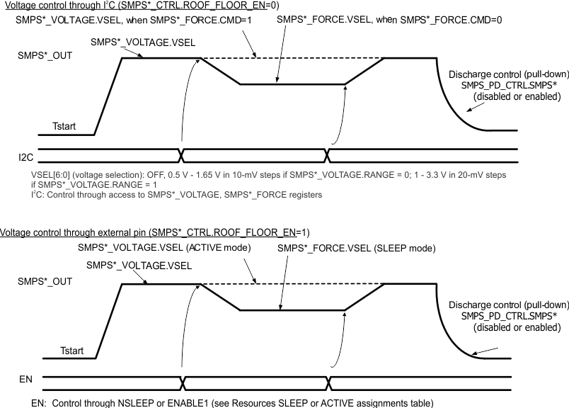
The step-down converters SMPS12 or SMPS123, SMPS45 or SMPS457, SMPS6, and SMPS8 are DVS-capable and have some additional parameters for control. The slew rate of the output voltage during voltage level change is fixed at 2.5 mV/µs. The control for two different voltage levels (ROOF and FLOOR) with the NSLEEP and ENABLE1 signals is available. When the ROOF_FLOOR control is not used, two different voltage levels can be selected with the CMD bit in the SMPSx_FORCE register.
- The output voltage slew rate for achieving new output voltage value is fixed at 2.5 mV/μs.
- The NSLEEP and ENABLE1 terminals can be used for roof-floor control of SMPS. For roof-floor operation sets the SMPSx_CTRL.ROOF_FLOOR_EN register, and assign SMPS to NSLEEP and ENABLE1 in the NSLEEP_SMPS_ASSIGN and ENABLE1_SMPS_ASSIGN registers. When the controlling terminal is active, the SMPS output value is defined by the SMPSx_VOLTAGE register. When the controlling terminal is not active, the SMPS output value is defined by the SMPSx_FORCE register.
- Set the second value for the output voltage with the SMPSx_FORCE.VSEL register. A value of 0x0 disables the SMPS (OFF).
- Select which register, SMPSx_VOLTAGE or SMPSx_FORCE, to use with the SMPSx_FORCE.CMD bit. The default is the voltage setting of SMPSx_VOLTAGE. For the CMD bit to work, ensure that SMPSx_CTRL.ROOF_FLOOR_EN = 0.
Figure 6-5 shows the SMPS controls for DVS.
 Figure 6-5 DVS – SMPS Controls