ZHCSG94L August 2013 – February 2019 TPS659038-Q1 , TPS659039-Q1
PRODUCTION DATA.
- 1 器件概要
- 2 修订历史记录
- 3 Device Comparison
- 4 Pin Configuration and Functions
-
5 Specifications
- 5.1 Absolute Maximum Ratings
- 5.2 ESD Ratings
- 5.3 Recommended Operating Conditions
- 5.4 Thermal Information
- 5.5 Electrical Characteristics: Latch Up Rating
- 5.6 Electrical Characteristics: LDO Regulator
- 5.7 Electrical Characteristics: Dual-Phase (SMPS12 and SMPS45) and Triple-Phase (SMPS123 and SMPS457) Regulators
- 5.8 Electrical Characteristics: Stand-Alone Regulators (SMPS3, SMPS6, SMPS7, SMPS8, and SMPS9)
- 5.9 Electrical Characteristics: Reference Generator (Bandgap)
- 5.10 Electrical Characteristics: 16-MHz Crystal Oscillator, 32-kHz RC Oscillator, and Output Buffers
- 5.11 Electrical Characteristics: DC-DC Clock Sync
- 5.12 Electrical Characteristics: 12-Bit Sigma-Delta ADC
- 5.13 Electrical Characteristics: Thermal Monitoring and Shutdown
- 5.14 Electrical Characteristics: System Control Thresholds
- 5.15 Electrical Characteristics: Current Consumption
- 5.16 Electrical Characteristics: Digital Input Signal Parameters
- 5.17 Electrical Characteristics: Digital Output Signal Parameters
- 5.18 Electrical Characteristics: I/O Pullup and Pulldown Resistance
- 5.19 I2C Interface Timing Requirements
- 5.20 SPI Timing Requirements
- 5.21 Typical Characteristics
-
6 Detailed Description
- 6.1 Overview
- 6.2 Functional Block Diagrams
- 6.3
Feature Description
- 6.3.1 Power Management
- 6.3.2
Power Resources (Step-Down and Step-Up SMPS Regulators, LDOs)
- 6.3.2.1
Step-Down Regulators
- 6.3.2.1.1 Sync Clock Functionality
- 6.3.2.1.2 Output Voltage and Mode Selection
- 6.3.2.1.3 Current Monitoring and Short Circuit Detection
- 6.3.2.1.4 POWERGOOD
- 6.3.2.1.5 DVS-Capable Regulators
- 6.3.2.1.6 Non DVS-Capable Regulators
- 6.3.2.1.7 Step-Down Converters SMPS12 and SMPS123
- 6.3.2.1.8 Step-Down Converter SMPS45 and SMPS457
- 6.3.2.1.9 Step-Down Converters SMPS3, SMPS6, SMPS7, SMPS8, and SMPS9
- 6.3.2.2 LDOs – Low Dropout Regulators
- 6.3.2.1
Step-Down Regulators
- 6.3.3 Long-Press Key Detection
- 6.3.4 RTC
- 6.3.5 GPADC – 12-Bit Sigma-Delta ADC
- 6.3.6 General-Purpose I/Os (GPIO Terminals)
- 6.3.7 Thermal Monitoring
- 6.3.8 Interrupts
- 6.3.9 Control Interfaces
- 6.3.10 Device Identification
- 6.4 Device Functional Modes
-
7 Application and Implementation
- 7.1 Application Information
- 7.2
Typical Application
- 7.2.1 Design Requirements
- 7.2.2 Detailed Design Procedure
- 7.2.3 Application Curves
- 8 Power Supply Recommendations
- 9 Layout
- 10器件和文档支持
- 11机械、封装和可订购信息
6.4.3 Power Sequences
A power sequence is an automatic pre-programmed sequence handled by the TPS65903x-Q1 device series to configure the device resources: SMPSs, LDOs, 32-kHz clock, part of GPIOs, , REGEN signals) into on, off, or sleep modes. See Section 6.3.6 for GPIO details.
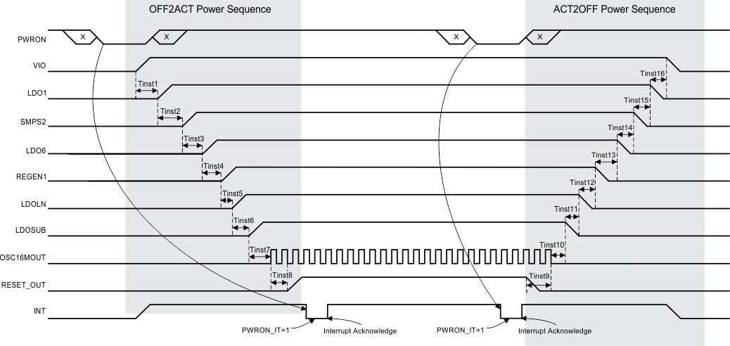
Figure 6-19 shows an example of an OFF2ACT transition followed by an ACT2OFF transition. The sequence is triggered through PWRON terminal and the resources controlled (for this example) are: VIO, LDO1, SMPS2, LDO6, REGEN1, LDOLN, LDOUSB, and CLK32KOUT. The time between each resource enable and disable (TinstX) is also part of the preprogrammed sequence definition.
When a resource is not assigned to any power sequence, it remains in off mode. The user (through software) can enable and configure this resource independently after the power sequence completes.
 Figure 6-19 Power Sequence Example
 The power sequences of the TPS65903x-Q1 device series are defined according to the processor requirements, see the relevant Application Note for more information.