ZHCSI09S June 2010 – August 2018 TPS65911
PRODUCTION DATA.
- 1器件概述
- 2修订历史记录
- 3Device Comparison Table
- 4Pin Configuration and Functions
-
5Specifications
- 5.1 Absolute Maximum Ratings
- 5.2 ESD Ratings
- 5.3 Recommended Operating Conditions
- 5.4 Thermal Information
- 5.5 Electrical Characteristics: I/O Pullup and Pulldown
- 5.6 Electrical Characteristics: Digital I/O Voltage
- 5.7 Electrical Characteristics: Power Consumption
- 5.8 Electrical Characteristics: Power References and Thresholds
- 5.9 Electrical Characteristics: Thermal Monitoring and Shutdown
- 5.10 Electrical Characteristics: 32-kHz RTC Clock
- 5.11 Electrical Characteristics: Backup Battery Charger
- 5.12 Electrical Characteristics: VRTC LDO
- 5.13 Electrical Characteristics: VIO SMPS
- 5.14 Electrical Characteristics: VDD1 SMPS
- 5.15 Electrical Characteristics: VDD2 SMPS
- 5.16 Electrical Characteristics: VDDCtrl SMPS
- 5.17 Electrical Characteristics: LDO1 and LDO2
- 5.18 Electrical Characteristics: LDO3 and LDO4
- 5.19 Electrical Characteristics: LDO5
- 5.20 Electrical Characteristics: LDO6, LDO7, and LDO8
- 5.21 Timing and Switching Characteristics
-
6Detailed Description
- 6.1 Overview
- 6.2 Functional Block Diagram
- 6.3 Power Reference
- 6.4 Power Resources
- 6.5 Embedded Power Controller (EPC)
- 6.6 PWM and LED Generators
- 6.7 Dynamic Voltage Frequency Scaling and Adaptive Voltage Scaling Operation
- 6.8 32-kHz RTC Clock
- 6.9 Real Time Clock (RTC)
- 6.10 Backup Battery Management
- 6.11 Backup Registers
- 6.12 I2C Interface
- 6.13 Thermal Monitoring and Shutdown
- 6.14 Interrupts
- 6.15 Register Maps
-
7Applications, Implementation, and Layout
- 7.1 Application Information
- 7.2 Typical Application
- 7.3 Power Supply Recommendations
- 8器件和文档支持
- 9机械、封装和可订购信息
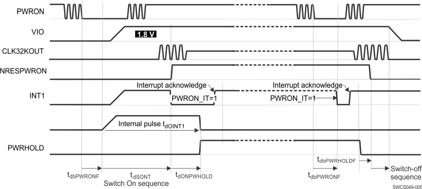
5.21.3.1 Device State Control Through PWRON Signal
Figure 5-2 shows the device state control through PWRON signal.

- The DEV_ON or AUTODEV_ON control bits can be used instead of the PWRHOLD signal to maintain supplies on after a switch-on sequence.
- The internal POWER ON enable condition pulse, tdOINT1, keeps device active until a PWRHOLD acknowledge.
- Switch-off from PWRHOLD removal.
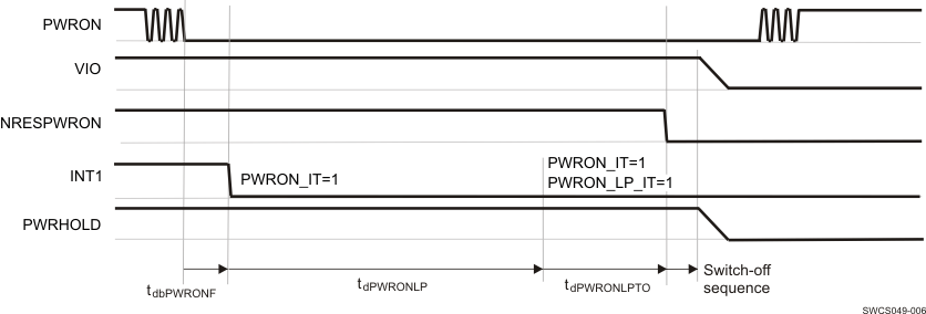
 Figure 5-3 PWRON Long-Press Turnoff
 Table 5-4 lists the power control timing characteristics.
Table 5-4 Power Control Timing Characteristics
| PARAMETER | TEST CONDITIONS | MIN | TYP | MAX | UNIT | |
|---|---|---|---|---|---|---|
| tdbPWRONF | PWRON falling-edge debouncing delay | 100 | ms | |||
| tdbPWRONR | PWRON rising-edge debouncing delay | 3 × tCK32k = 94 | µs | |||
| tdbPWRHOLD | PWRHOLD rising-edge debouncing delay | 2 × tCK32k = 63 | µs | |||
| tdOINT1 | INT1 (internal) power-on pulse duration after PWRON low-level (debounced) event | 1 | s | |||
| tdONPWHOLD | Delay to set high PWRHOLD signal or DEV_ON control bit after NRESPWON released to keep on the supplies | tdOINT1 – tDSONT = 970(1) | ms | |||
| tdPWRONLP | PWRON long-press delay | PWRON falling-edge to PWRON_LP_IT | 4 | s | ||
| tdPWRONLPTO | PWROW long-press interrupt (PWRON_LP_IT) to supplies switch-off | PWRON_LP_IT to NRESPWRON falling-edge | 1 | s | ||
(1) TdSONT = 30 ms, as in example boot sequence.