ZHCSI09S June   2010  – August 2018 TPS65911

PRODUCTION DATA.  

  1. 1器件概述
    1. 1.1 特性
    2. 1.2 应用
    3. 1.3 说明
    4. 1.4 功能方框图
  2. 2修订历史记录
  3. 3Device Comparison Table
  4. 4Pin Configuration and Functions
    1. 4.1 Pin Attributes
      1.      Pin Attributes
  5. 5Specifications
    1. 5.1  Absolute Maximum Ratings
    2. 5.2  ESD Ratings
    3. 5.3  Recommended Operating Conditions
    4. 5.4  Thermal Information
    5. 5.5  Electrical Characteristics: I/O Pullup and Pulldown
    6. 5.6  Electrical Characteristics: Digital I/O Voltage
    7. 5.7  Electrical Characteristics: Power Consumption
    8. 5.8  Electrical Characteristics: Power References and Thresholds
    9. 5.9  Electrical Characteristics: Thermal Monitoring and Shutdown
    10. 5.10 Electrical Characteristics: 32-kHz RTC Clock
    11. 5.11 Electrical Characteristics: Backup Battery Charger
    12. 5.12 Electrical Characteristics: VRTC LDO
    13. 5.13 Electrical Characteristics: VIO SMPS
    14. 5.14 Electrical Characteristics: VDD1 SMPS
    15. 5.15 Electrical Characteristics: VDD2 SMPS
    16. 5.16 Electrical Characteristics: VDDCtrl SMPS
    17. 5.17 Electrical Characteristics: LDO1 and LDO2
    18. 5.18 Electrical Characteristics: LDO3 and LDO4
    19. 5.19 Electrical Characteristics: LDO5
    20. 5.20 Electrical Characteristics: LDO6, LDO7, and LDO8
    21. 5.21 Timing and Switching Characteristics
      1. 5.21.1 I2C Timing and Switching
      2. 5.21.2 Switch-ON and Switch-OFF Sequences and Timing
      3. 5.21.3 Power Control Timing
        1. 5.21.3.1 Device State Control Through PWRON Signal
        2. 5.21.3.2 Device SLEEP State Control
        3. 5.21.3.3 Device Turnon and Turnoff With Rising and Falling Input Voltage
        4. 5.21.3.4 Power Supplies State Control Through EN1 and EN2 Signals
        5. 5.21.3.5 VDD1, VDD2 Voltage Control Through EN1 and EN2 Signals
  6. 6Detailed Description
    1. 6.1  Overview
    2. 6.2  Functional Block Diagram
    3. 6.3  Power Reference
    4. 6.4  Power Resources
    5. 6.5  Embedded Power Controller (EPC)
      1. 6.5.1 State Machine
        1. 6.5.1.1 Device POWER ON Enable Conditions
        2. 6.5.1.2 Device POWER ON Disable Conditions
        3. 6.5.1.3 Device SLEEP Enable Conditions
        4. 6.5.1.4 Device Reset Scenarios
      2. 6.5.2 BOOT Configuration, Switch-ON, and Switch-OFF Sequences
      3. 6.5.3 Control Signals
        1. 6.5.3.1  SLEEP
        2. 6.5.3.2  PWRHOLD
        3. 6.5.3.3  BOOT1
        4. 6.5.3.4  NRESPWRON, NRESPWRON2
        5. 6.5.3.5  CLK32KOUT
        6. 6.5.3.6  PWRON
        7. 6.5.3.7  INT1
        8. 6.5.3.8  EN2 and EN1
        9. 6.5.3.9  GPIO0 to GPIO8
        10. 6.5.3.10 HDRST Input
        11. 6.5.3.11 PWRDN
        12. 6.5.3.12 Comparators: COMP1 and COMP2
        13. 6.5.3.13 Watchdog
        14. 6.5.3.14 Tracking LDO
    6. 6.6  PWM and LED Generators
    7. 6.7  Dynamic Voltage Frequency Scaling and Adaptive Voltage Scaling Operation
    8. 6.8  32-kHz RTC Clock
    9. 6.9  Real Time Clock (RTC)
      1. 6.9.1 Time Calendar Registers
      2. 6.9.2 General Registers
      3. 6.9.3 Compensation Registers
    10. 6.10 Backup Battery Management
    11. 6.11 Backup Registers
    12. 6.12 I2C Interface
      1. 6.12.1 Access Protocols
        1. 6.12.1.1 Single Byte Access
        2. 6.12.1.2 Multiple Byte Access to Several Adjacent Registers
    13. 6.13 Thermal Monitoring and Shutdown
    14. 6.14 Interrupts
    15. 6.15 Register Maps
      1. 6.15.1 Functional Registers
        1. 6.15.1.1 TPS65911_FUNC_REG Registers Mapping Summary
        2. 6.15.1.2 TPS65911_FUNC_REG Register Descriptions
  7. 7Applications, Implementation, and Layout
    1. 7.1 Application Information
    2. 7.2 Typical Application
      1. 7.2.1 Design Requirements
      2. 7.2.2 Detailed Design Procedure
        1. 7.2.2.1 External Component Recommendation
        2. 7.2.2.2 Controller Design Procedure
          1. 7.2.2.2.1 Inductor Selection
          2. 7.2.2.2.2 Selecting the RTRIP Resistor
          3. 7.2.2.2.3 Selecting the Output Capacitors
          4. 7.2.2.2.4 Selecting FETs
          5. 7.2.2.2.5 Bootstrap Capacitor
          6. 7.2.2.2.6 Selecting Input Capacitors
        3. 7.2.2.3 Converter Design Procedure
          1. 7.2.2.3.1 Selecting the Inductor
          2. 7.2.2.3.2 Selecting Output Capacitors
          3. 7.2.2.3.3 Selecting Input Capacitors
      3. 7.2.3 Application Curves
      4. 7.2.4 Layout Guidelines
        1. 7.2.4.1 PCB Layout
      5. 7.2.5 Layout Example
    3. 7.3 Power Supply Recommendations
  8. 8器件和文档支持
    1. 8.1 器件支持
      1. 8.1.1 开发支持
      2. 8.1.2 器件命名规则
    2. 8.2 文档支持
      1. 8.2.1 相关文档
    3. 8.3 接收文档更新通知
    4. 8.4 社区资源
      1. 8.4.1 社区资源
    5. 8.5 商标
    6. 8.6 静电放电警告
    7. 8.7 术语表
  9. 9机械、封装和可订购信息
    1. 9.1 封装 说明

封装选项

机械数据 (封装 | 引脚)
散热焊盘机械数据 (封装 | 引脚)
订购信息

Real Time Clock (RTC)

The RTC, which is driven by the 32-kHz clock, provides the alarm and timekeeping functions. The RTC is kept supplied when the device is in the OFF state or the BACKUP state.

The primary functions of the RTC block are:

  • Time information (seconds/minutes/hours) directly in binary-coded decimal (BCD) format
  • Calendar information (Day/Month/Year/Day of the week) directly in BCD code up to year 2099
  • Programmable interrupts generation: The RTC can generate two interrupts: a timer interrupt RTC_PERIOD_IT periodically (1s/1m/1h/1d period) and an alarm interrupt RTC_ALARM_IT at a precise time of the day (alarm function). These interrupts are enabled using IT_ALARM and IT_TIMER control bits. Periodically interrupts can be masked during the SLEEP period to avoid host interruption and are automatically unmasked after SLEEP wakeup (using the IT_SLEEP_MASK_EN control bit).
  • Oscillator frequency calibration and time correction
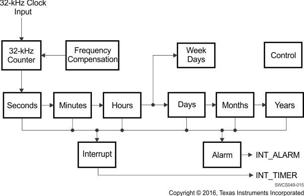
TPS65911 SWCS049-015.gifFigure 6-5 RTC Digital Section Block Diagram