SWCS071C August 2012 – August 2017
PRODUCTION DATA.
- 1 Device Overview
- 2 Revision History
- 3 Default Settings
- 4 Pin Configuration and Functions
-
5 Specifications
- 5.1 Absolute Maximum Ratings
- 5.2 ESD Ratings
- 5.3 Recommended Operating Conditions
- 5.4 Thermal Characteristics
- 5.5 Electrical Characteristics - DCDC1, DCDC2, and DCDC3
- 5.6 Electrical Characteristics - DCDC4
- 5.7 Electrical Characteristics - LDOs
- 5.8 Electrical Characteristics - Digital Inputs, Digital Outputs
- 5.9 Electrical Characteristics - VMON Voltage Monitor, VDDIO, Undervoltage Lockout (UVLO), and LDOAO
- 5.10 Electrical Characteristics - Load Switch
- 5.11 Electrical Characteristics - LED Drivers
- 5.12 Electrical Characteristics - Thermal Monitoring and Shutdown
- 5.13 Electrical Characteristics - 32-kHz RC Clock
- 5.14 SPI Interface Timing Requirements
- 5.15 I2C Interface Timing Requirements
- 5.16 Typical Characteristics
- 6 Parameter Measurement Information
-
7 Detailed Description
- 7.1 Overview
- 7.2 Functional Block Diagram
- 7.3 Linear Regulators
- 7.4 Step-Down Converters
- 7.5 GPIOs
- 7.6 Power State Machine
- 7.7 Transition Conditions
- 7.8 Implementation of Internal Power-Up and Power-Down Sequencing
- 7.9 EN1, EN2, EN3, EN4, Resources Control
- 7.10 SLEEP State Control
- 7.11 Registers SET_OFF, KEEP_ON and DEF_VOLT Used in SLEEP State; CONFIG2 = 1
- 7.12 Registers SET_OFF, KEEP_ON and DEF_VOLT Used for Resources Assigned to an External Enable Pin; CONFIG2 = 1
- 7.13 Registers SET_OFF, KEEP_ON and DEF_VOLT for Resources Assigned to Pins PWR_REQ, CLK_REQ1 and CLK_REQ2; CONFIG2 = 0
- 7.14 Voltage Scaling Interface Control Using _OP and _AVS Registers with I2C or SPI Interface
- 7.15 Voltage Scaling Using the VCON Decoder on Pins VCON_PWM and VCON_CLK
- 7.16 Configuration Pins CONFIG1, CONFIG2 and DEF_SPI_I2C-GPIO
- 7.17 VDDIO Voltage for Push-Pull Output Stages
- 7.18 Digital Signal Summary
- 7.19 TPS659121 On/Off Operation With E450, E500
- 7.20 TPS659122 On/Off Operation for CONFIG1=HIGH
- 7.21 TPS659122 On/Off Operation for CONFIG1=LOW
- 7.22 Interfaces
- 7.23 Serial Peripheral Interface
- 7.24 I2C Interface
- 7.25 Thermal Monitoring and Shutdown
- 7.26 Load Switch
- 7.27 LED Driver
- 7.28
Memory
- 7.28.1 Register Format
- 7.28.2
Register Descriptions
- 7.28.2.1
DCDC Registers
- 7.28.2.1.1 DCDC1_CTRL (00h)
- 7.28.2.1.2 DCDC2_CTRL (01h)
- 7.28.2.1.3 DCDC3_CTRL (02h)
- 7.28.2.1.4 DCDC4_CTRL (03h)
- 7.28.2.1.5 DCDC1_OP (04h)
- 7.28.2.1.6 DCDC1_AVS (05h)
- 7.28.2.1.7 DCDC1_LIMIT (06h)
- 7.28.2.1.8 DCDC2_OP (07h)
- 7.28.2.1.9 DCDC2_AVS (08h)
- 7.28.2.1.10 DCDC2_LIMIT (09h)
- 7.28.2.1.11 DCDC3_OP (0Ah)
- 7.28.2.1.12 DCDC3_AVS (0Bh)
- 7.28.2.1.13 DCDC3_LIMIT (0Ch)
- 7.28.2.1.14 DCDC4_OP (0Dh)
- 7.28.2.1.15 DCDC4_AVS (0Eh)
- 7.28.2.1.16 DCDC4_LIMIT (0Fh)
- 7.28.2.1.17 VDCDCx Range Settings
- 7.28.2.1.18 DCDCx Voltage Settings
- 7.28.2.2
LDO Registers
- 7.28.2.2.1 LDO1_OP (10h)
- 7.28.2.2.2 LDO1_AVS (11h)
- 7.28.2.2.3 LDO1_LIMIT (12h)
- 7.28.2.2.4 LDO2_OP (13h)
- 7.28.2.2.5 LDO2_AVS (14h)
- 7.28.2.2.6 LDO2_LIMIT (15h)
- 7.28.2.2.7 LDO3_OP (16h)
- 7.28.2.2.8 LDO3_AVS (17h)
- 7.28.2.2.9 LDO3_LIMIT (18h)
- 7.28.2.2.10 LDO4_OP (19h)
- 7.28.2.2.11 LDO4_AVS (1Ah)
- 7.28.2.2.12 LDO4_LIMIT (1Bh)
- 7.28.2.2.13 LDO5 (1Ch)
- 7.28.2.2.14 LDO6 (1Dh)
- 7.28.2.2.15 LDO7 (1Eh)
- 7.28.2.2.16 LDO8 (1Fh)
- 7.28.2.2.17 LDO9 (20h)
- 7.28.2.2.18 LDO10 (21h)
- 7.28.2.3 LDO Voltage Settings
- 7.28.2.4
DEVCTRL Registers
- 7.28.2.4.1 THRM_REG (22h)
- 7.28.2.4.2 CLK32KOUT (23h)
- 7.28.2.4.3 DEVCTRL (24h)
- 7.28.2.4.4 DEVCTRL2 (25h)
- 7.28.2.4.5 I2C_SPI_CFG (26h)
- 7.28.2.4.6 KEEP_ON1 (27h)
- 7.28.2.4.7 KEEP_ON2 (28h)
- 7.28.2.4.8 SET_OFF1 (29h)
- 7.28.2.4.9 SET_OFF2 (2Ah)
- 7.28.2.4.10 DEF_VOLT (2Bh)
- 7.28.2.4.11 LDO Sleep Mode Behavior
- 7.28.2.4.12 DEF_VOLT_MAPPING (2Ch)
- 7.28.2.4.13 DISCHARGE1 (2Dh)
- 7.28.2.4.14 DISCHARGE2 (2Eh)
- 7.28.2.4.15 EN1_SET1 (2Fh)
- 7.28.2.4.16 EN1_SET2 (30h)
- 7.28.2.4.17 EN2_SET1 (31h)
- 7.28.2.4.18 EN2_SET2 (32h)
- 7.28.2.4.19 EN3_SET1 (33h)
- 7.28.2.4.20 EN3_SET2 (34h)
- 7.28.2.4.21 EN4_SET1 (35h)
- 7.28.2.4.22 EN4_SET2 (36h)
- 7.28.2.4.23 PGOOD (37h)
- 7.28.2.4.24 PGOOD2 (38h)
- 7.28.2.4.25 INT_STS (39h)
- 7.28.2.4.26 INT_MSK (3Ah)
- 7.28.2.4.27 INT_STS2 (3Bh)
- 7.28.2.4.28 INT_MSK2 (3Ch)
- 7.28.2.4.29 INT_STS3 (3Dh)
- 7.28.2.4.30 INT_MSK3 (3Eh)
- 7.28.2.4.31 INT_STS4 (3Fh)
- 7.28.2.4.32 INT_MSK4 (40h)
- 7.28.2.4.33 GPIO1 (41h)
- 7.28.2.4.34 GPIO2 (42h)
- 7.28.2.4.35 GPIO3 (43h)
- 7.28.2.4.36 GPIO4 (44h)
- 7.28.2.4.37 GPIO5 (45h)
- 7.28.2.4.38 VMON (46h)
- 7.28.2.4.39 LEDA_CTRL1 (47h)
- 7.28.2.4.40 LEDA_CTRL2 (48h)
- 7.28.2.4.41 LEDA_CTRL3 (49h)
- 7.28.2.4.42 LEDA_CTRL4 (4Ah)
- 7.28.2.4.43 LEDA_CTRL5 (4Bh)
- 7.28.2.4.44 LEDA_CTRL6 (4Ch)
- 7.28.2.4.45 LEDA_CTRL7 (4Dh)
- 7.28.2.4.46 LEDA_CTRL8 (4Eh)
- 7.28.2.4.47 LEDB_CTRL1 (4Fh)
- 7.28.2.4.48 LEDB_CTRL2 (50h)
- 7.28.2.4.49 LEDB_CTRL3 (51h)
- 7.28.2.4.50 LEDB_CTRL4 (52h)
- 7.28.2.4.51 LEDB_CTRL5 (53h)
- 7.28.2.4.52 LEDB_CTRL6 (54h)
- 7.28.2.4.53 LEDB_CTRL7 (55h)
- 7.28.2.4.54 LEDB_CTRL8 (56h)
- 7.28.2.4.55 LEDC_CTRL1 (57h)
- 7.28.2.4.56 LEDC_CTRL2 (58h)
- 7.28.2.4.57 LEDC_CTRL3 (59h)
- 7.28.2.4.58 LED_CTRL4 (5Ah)
- 7.28.2.4.59 LEDC_CTRL5 (5Bh)
- 7.28.2.4.60 LEDC_CTRL6 (5Ch)
- 7.28.2.4.61 LEDC_CTRL7 (5Dh)
- 7.28.2.4.62 LEDC_CTRL8 (5Eh)
- 7.28.2.4.63 LED_RAMP_UP_TIME (5Fh)
- 7.28.2.4.64 LED_RAMP_DOWN_TIME (60h)
- 7.28.2.4.65 LED_SEQ_EN (61h)
- 7.28.2.4.66 LEDx DC Current
- 7.28.2.4.67 LOADSWITCH (62h)
- 7.28.2.4.68 SPARE (63h)
- 7.28.2.4.69 VERNUM (64h)
- 7.28.2.1
DCDC Registers
- 8 Applications, Implementation, and Layout
- 9 Device and Documentation Support
- 10Mechanical, Packaging, and Orderable Information
6 Parameter Measurement Information
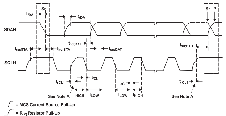
6.1 I2C Timing Diagrams
 Figure 6-1 Serial Interface Timing Diagram for FS-Mode

A. First rising edge of the SCLH signal after Sr and after each acknowledge bit.
Figure 6-2 Serial Interface Timing Diagram for HS-Mode
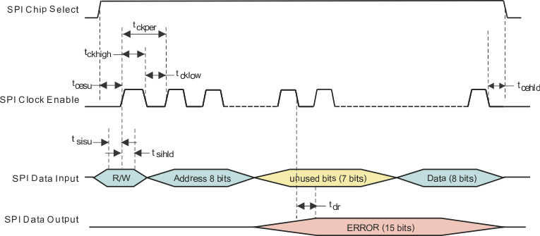
6.2 SPI Timing Diagram
 Figure 6-3 SPI Interface Timing