ZHCSFH6C March 2016 – February 2019 TPS65916
PRODUCTION DATA.
- 1器件概述
- 2修订历史记录
- 3Pin Configuration and Functions
-
4Specifications
- 4.1 Absolute Maximum Ratings
- 4.2 ESD Ratings
- 4.3 Recommended Operating Conditions
- 4.4 Thermal Information
- 4.5 Electrical Characteristics — LDO Regulators
- 4.6 Electrical Characteristics — SMPS1&2 in Dual-Phase Configuration
- 4.7 Electrical Characteristics — SMPS1, SMPS2, SMPS3, SMPS4, and SMPS5 Stand-Alone Regulators
- 4.8 Electrical Characteristics — Reference Generator (Bandgap)
- 4.9 Electrical Characteristics — 32-kHz RC Oscillators and SYNCCLKOUT Output Buffers
- 4.10 Electrical Characteristics — 12-Bit Sigma-Delta ADC
- 4.11 Electrical Characteristics — Thermal Monitoring and Shutdown
- 4.12 Electrical Characteristics — System Control Thresholds
- 4.13 Electrical Characteristics — Current Consumption
- 4.14 Electrical Characteristics — Digital Input Signal Parameters
- 4.15 Electrical Characteristics — Digital Output Signal Parameters
- 4.16 I/O Pullup and Pulldown Characteristics
- 4.17 Electrical Characteristics — I2C Interface
- 4.18 Timing Requirements — I2C Interface
- 4.19 Timing Requirements — SPI
- 4.20 Switching Characteristics — LDO Regulators
- 4.21 Switching Characteristics — SMPS1&2 in Dual-Phase Configuration
- 4.22 Switching Characteristics — SMPS1, SMPS2, SMPS3, SMPS4, and SMPS5 Stand-Alone Regulators
- 4.23 Switching Characteristics — Reference Generator (Bandgap)
- 4.24 Switching Characteristics — PLL for SMPS Clock Generation
- 4.25 Switching Characteristics — 32-kHz RC Oscillators and SYNCCLKOUT Output Buffers
- 4.26 Switching Characteristics — 12-Bit Sigma-Delta ADC
- 4.27 Typical Characteristics
-
5Detailed Description
- 5.1 Overview
- 5.2 Functional Block Diagram
- 5.3 Device State Machine
- 5.4
Power Resources (Step-Down and Step-Up SMPS Regulators, LDOs)
- 5.4.1 Step-Down Regulators
- 5.4.2 Low Dropout Regulators (LDOs)
- 5.5 SMPS and LDO Input Supply Connections
- 5.6 First Supply Detection
- 5.7 Long-Press Key Detection
- 5.8 12-Bit Sigma-Delta General-Purpose ADC (GPADC)
- 5.9 General-Purpose I/Os (GPIO Pins)
- 5.10 Thermal Monitoring
- 5.11 Interrupts
- 5.12 Control Interfaces
- 5.13 OTP Configuration Memory
- 5.14 Watchdog Timer (WDT)
- 5.15 System Voltage Monitoring
- 5.16 Register Map
- 5.17 Device Identification
- 6Applications, Implementation, and Layout
- 7器件和文档支持
- 8机械、封装和可订购信息
6.2.2.6.2 Maintaining Sufficient Input Voltage
In the event of high loading during loss of input voltage, there is a risk to go below the voltage level necessary for the internal logic of the device to work properly before the device is disabled. This means that when the VCCA voltage supply level becomes lower than the VSYS_LO threshold, the input voltage may continue dropping to very low voltages during the 180 us ±10% delay before the device is disabled.
If a large input voltage drop occurs before the device is disabled, the internal logic can no longer properly drive the FETs of the SMPS, and it is possible that the high-side FET and low-side FET of the SMPS are on at the same time. In the event that the high-side and low-side FETs for an SMPS are on at the same time, there is a direct path from SMPSx_IN to GND, allowing cross-conduction and possible damage of the device.
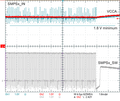
In order to prevent damage or irregular switching behavior, it is important that the voltage at the SMPSx_IN pin stays above 1.8 V, including negative transients, before the device is disabled. The minimum voltage seen at the SMPSx_IN pin is dependent on VCCA and the PCB inductance between the SMPSx_IN pin and the input capacitor. Use Equation 2 to determine the minimum capacitance needed on VCCA to ensure that the device continues switching properly before it is disabled.
where
- C is total capacitance on VCCA, including preregulator output capacitance and PMIC input capacitance
- I is the total current on the PMIC input supply
- ΔT is the maximum debounce time after VCCA = VSYS_LO before the device switches off (198us)
- VSYS_LO is the threshold where the device is disabled
- VCCAMIN is the minimum VCCA voltage to keep the SMPSx_IN transients above 1.8 V
When measuring the SMPSx_IN and VCCA during power down, use active differential probes and a high resolution oscilloscope (4GS/sec or more). VCCA can be measured over the 10uF input capacitor. However, SMPSx_IN must be measured at the pin in order to measure the transients on this rail accurately. To measure SMPSx_IN, place the negative lead of the differential probe at a nearby GND, such as the GND of the SMPSx_IN input capacitor. Place the positive lead of the differential probe directly on the exposed metal of the SMPSx_IN pin. With this set up, verify that SMPSx_IN, including the ripple on this signal, does not drop below 1.8V before the SMPS stops switching. See Figure 6-4 for an example of how to take this measurement. For ways to decrease the amplitude of the transient spikes, see Table 6-3 for recommended parasitic inductance requirements.
 Figure 6-4 Waveform of SMPSx_IN Transients