ZHCSFH6C March   2016  – February 2019 TPS65916

PRODUCTION DATA.  

  1. 1器件概述
    1. 1.1 特性
    2. 1.2 应用
    3. 1.3 说明
    4. 1.4 功能图
  2. 2修订历史记录
  3. 3Pin Configuration and Functions
    1. 3.1 Pin Attributes
      1.      Pin Attributes
    2. 3.2 Signal Descriptions
  4. 4Specifications
    1. 4.1  Absolute Maximum Ratings
    2. 4.2  ESD Ratings
    3. 4.3  Recommended Operating Conditions
    4. 4.4  Thermal Information
    5. 4.5  Electrical Characteristics — LDO Regulators
    6. 4.6  Electrical Characteristics — SMPS1&2 in Dual-Phase Configuration
    7. 4.7  Electrical Characteristics — SMPS1, SMPS2, SMPS3, SMPS4, and SMPS5 Stand-Alone Regulators
    8. 4.8  Electrical Characteristics — Reference Generator (Bandgap)
    9. 4.9  Electrical Characteristics — 32-kHz RC Oscillators and SYNCCLKOUT Output Buffers
    10. 4.10 Electrical Characteristics — 12-Bit Sigma-Delta ADC
    11. 4.11 Electrical Characteristics — Thermal Monitoring and Shutdown
    12. 4.12 Electrical Characteristics — System Control Thresholds
    13. 4.13 Electrical Characteristics — Current Consumption
    14. 4.14 Electrical Characteristics — Digital Input Signal Parameters
    15. 4.15 Electrical Characteristics — Digital Output Signal Parameters
    16. 4.16 I/O Pullup and Pulldown Characteristics
    17. 4.17 Electrical Characteristics — I2C Interface
    18. 4.18 Timing Requirements — I2C Interface
    19. 4.19 Timing Requirements — SPI
    20. 4.20 Switching Characteristics — LDO Regulators
    21. 4.21 Switching Characteristics — SMPS1&2 in Dual-Phase Configuration
    22. 4.22 Switching Characteristics — SMPS1, SMPS2, SMPS3, SMPS4, and SMPS5 Stand-Alone Regulators
    23. 4.23 Switching Characteristics — Reference Generator (Bandgap)
    24. 4.24 Switching Characteristics — PLL for SMPS Clock Generation
    25. 4.25 Switching Characteristics — 32-kHz RC Oscillators and SYNCCLKOUT Output Buffers
    26. 4.26 Switching Characteristics — 12-Bit Sigma-Delta ADC
    27. 4.27 Typical Characteristics
  5. 5Detailed Description
    1. 5.1  Overview
    2. 5.2  Functional Block Diagram
    3. 5.3  Device State Machine
      1. 5.3.1  Embedded Power Controller
      2. 5.3.2  State Transition Requests
        1. 5.3.2.1 ON Requests
        2. 5.3.2.2 OFF Requests
        3. 5.3.2.3 SLEEP and WAKE Requests
      3. 5.3.3  Power Sequences
      4. 5.3.4  Device Power Up Timing
      5. 5.3.5  Power-On Acknowledge
        1. 5.3.5.1 POWERHOLD Mode
        2. 5.3.5.2 AUTODEVON Mode
      6. 5.3.6  BOOT Configuration
        1. 5.3.6.1 Boot Pin Usage and Connection
      7. 5.3.7  Reset Levels
      8. 5.3.8  INT
      9. 5.3.9  Warm Reset
      10. 5.3.10 RESET_IN
    4. 5.4  Power Resources (Step-Down and Step-Up SMPS Regulators, LDOs)
      1. 5.4.1 Step-Down Regulators
        1. 5.4.1.1 Output Voltage and Mode Selection
        2. 5.4.1.2 Clock Generation for SMPS
        3. 5.4.1.3 Current Monitoring and Short Circuit Detection
        4. 5.4.1.4 POWERGOOD
        5. 5.4.1.5 DVS-Capable Regulators
          1. 5.4.1.5.1 Non DVS-Capable Regulators
        6. 5.4.1.6 Step-Down Converters SMPS1, SMPS2 or SMPS1&2
        7. 5.4.1.7 Step-Down Converters SMPS3, SMPS4, and SMPS5
      2. 5.4.2 Low Dropout Regulators (LDOs)
        1. 5.4.2.1 LDOVANA
        2. 5.4.2.2 LDOVRTC
        3. 5.4.2.3 LDO1 and LDO2
        4. 5.4.2.4 Low-Noise LDO (LDO5)
        5. 5.4.2.5 Other LDOs
    5. 5.5  SMPS and LDO Input Supply Connections
    6. 5.6  First Supply Detection
    7. 5.7  Long-Press Key Detection
    8. 5.8  12-Bit Sigma-Delta General-Purpose ADC (GPADC)
      1. 5.8.1 Asynchronous Conversion Request (SW)
      2. 5.8.2 Periodic Conversion (AUTO)
      3. 5.8.3 Calibration
    9. 5.9  General-Purpose I/Os (GPIO Pins)
    10. 5.10 Thermal Monitoring
      1. 5.10.1 Hot-Die Function (HD)
      2. 5.10.2 Thermal Shutdown
    11. 5.11 Interrupts
    12. 5.12 Control Interfaces
      1. 5.12.1 I2C Interfaces
        1. 5.12.1.1 I2C Implementation
        2. 5.12.1.2 F/S Mode Protocol
        3. 5.12.1.3 HS Mode Protocol
      2. 5.12.2 Serial Peripheral Interface (SPI)
        1. 5.12.2.1 SPI Modes
        2. 5.12.2.2 SPI Protocol
    13. 5.13 OTP Configuration Memory
    14. 5.14 Watchdog Timer (WDT)
    15. 5.15 System Voltage Monitoring
    16. 5.16 Register Map
      1. 5.16.1 Functional Register Mapping
    17. 5.17 Device Identification
  6. 6Applications, Implementation, and Layout
    1. 6.1 Application Information
    2. 6.2 Typical Application
      1. 6.2.1 Design Requirements
      2. 6.2.2 Detailed Design Procedure
        1. 6.2.2.1 SMPS Input Capacitors
        2. 6.2.2.2 SMPS Output Capacitors
        3. 6.2.2.3 SMPS Inductors
        4. 6.2.2.4 LDO Input Capacitors
        5. 6.2.2.5 LDO Output Capacitors
        6. 6.2.2.6 VCCA
          1. 6.2.2.6.1 Meeting the Power-Down Sequence
          2. 6.2.2.6.2 Maintaining Sufficient Input Voltage
        7. 6.2.2.7 VIO_IN
        8. 6.2.2.8 GPADC
      3. 6.2.3 Application Curves
    3. 6.3 Layout
      1. 6.3.1 Layout Guidelines
      2. 6.3.2 Layout Example
    4. 6.4 Power Supply Coupling and Bulk Capacitors
  7. 7器件和文档支持
    1. 7.1 器件支持
      1. 7.1.1 第三方米6体育平台手机版_好二三四免责声明
      2. 7.1.2 器件命名规则
    2. 7.2 文档支持
      1. 7.2.1 相关文档
    3. 7.3 接收文档更新通知
    4. 7.4 社区资源
    5. 7.5 商标
    6. 7.6 静电放电警告
    7. 7.7 Glossary
  8. 8机械、封装和可订购信息

封装选项

机械数据 (封装 | 引脚)
散热焊盘机械数据 (封装 | 引脚)
订购信息

Typical Characteristics

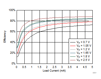
TPS65916 D001_slvsco4.gif
VI = 3.8 V ƒS = 2.2 MHz TA = 25°C
Figure 4-4 SMPS Efficiency for all SMPS in Eco-mode
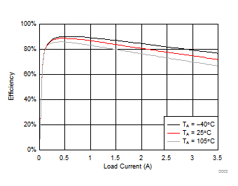
TPS65916 D003_slvsco4.gif
VI = 3.8 V ƒS = 2.2 MHz VO = 1.8 V
Figure 4-6 SMPS Efficiency for SMPS1 and SMPS2
in Single-Phase PWM Mode With Temperature Variation
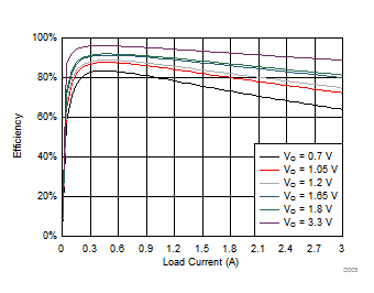
TPS65916 D005_slvsco4.gif
VI = 3.8 V ƒS = 2.2 MHz TA = 25°C
Figure 4-8 SMPS Efficiency for SMPS3
in PWM Mode
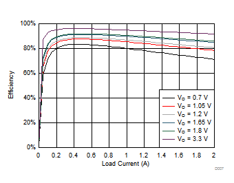
TPS65916 D007_slvsco4.gif
VI = 3.8 V ƒS = 2.2 MHz TA = 25°C
Figure 4-10 SMPS Efficiency for SMPS5
in PWM Mode
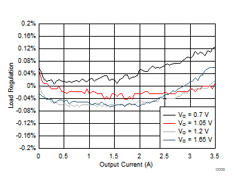
TPS65916 D009_slvsco4.gif
VI = 3.8 V ƒS = 2.2 MHz TA = 25°C
Figure 4-12 SMPS Load Regulation for SMPS1 and SMPS2 Single-Phase PWM Mode
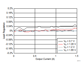
TPS65916 D010_slvsco4.gif
VI = 3.8 V ƒS = 2.2 MHz TA = 25°C
Figure 4-14 SMPS Load Regulation for SMPS4
in PWM Mode
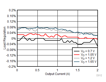
TPS65916 D012_slvsco4.gif
VI = 3.8 V ƒS = 2.2 MHz TA = 25°C
Figure 4-16 SMPS Load Regulation for SMPS5
in PWM Mode
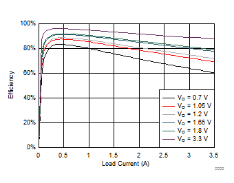
TPS65916 D002_slvsco4.gif
VI = 3.8 V ƒS = 2.2 MHz TA = 25°C
Figure 4-5 SMPS Efficiency for SMPS1 and SMPS2
in Single-Phase PWM Mode
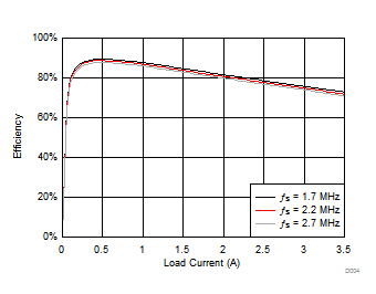
TPS65916 D004_slvsco4.gif
VI = 3.8 V VO = 1.8 V TA = 25°C
Figure 4-7 SMPS Efficiency for SMPS1 and SMPS2
in Single-Phase PWM Mode With Frequency Variation
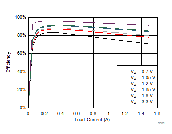
TPS65916 D006_slvsco4.gif
VI = 3.8 V ƒS = 2.2 MHz TA = 25°C
Figure 4-9 SMPS Efficiency for SMPS4
in PWM Mode
TPS65916 D008_slvsco4.gif
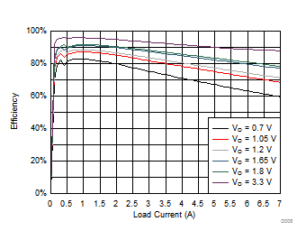
VI = 3.8 V ƒS = 2.2 MHz TA = 25°C
Figure 4-11 SMPS Efficiency for SMPS12
in Dual-Phase PWM Mode
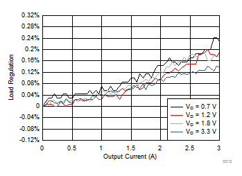
TPS65916 D013_slvsco4.gif
VI = 3.8 V ƒS = 2.2 MHz TA = 25°C
Figure 4-13 SMPS Load Regulation for SMPS3, PWM Mode
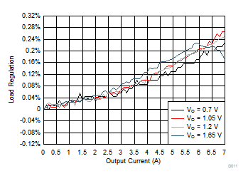
TPS65916 D011_slvsco4.gif
VI = 3.8 V ƒS = 2.2 MHz TA = 25°C
Figure 4-15 SMPS Load Regulation for SMPS12
in Dual-Phase PWM Mode