ZHCSFH6C March 2016 – February 2019 TPS65916
PRODUCTION DATA.
- 1器件概述
- 2修订历史记录
- 3Pin Configuration and Functions
-
4Specifications
- 4.1 Absolute Maximum Ratings
- 4.2 ESD Ratings
- 4.3 Recommended Operating Conditions
- 4.4 Thermal Information
- 4.5 Electrical Characteristics — LDO Regulators
- 4.6 Electrical Characteristics — SMPS1&2 in Dual-Phase Configuration
- 4.7 Electrical Characteristics — SMPS1, SMPS2, SMPS3, SMPS4, and SMPS5 Stand-Alone Regulators
- 4.8 Electrical Characteristics — Reference Generator (Bandgap)
- 4.9 Electrical Characteristics — 32-kHz RC Oscillators and SYNCCLKOUT Output Buffers
- 4.10 Electrical Characteristics — 12-Bit Sigma-Delta ADC
- 4.11 Electrical Characteristics — Thermal Monitoring and Shutdown
- 4.12 Electrical Characteristics — System Control Thresholds
- 4.13 Electrical Characteristics — Current Consumption
- 4.14 Electrical Characteristics — Digital Input Signal Parameters
- 4.15 Electrical Characteristics — Digital Output Signal Parameters
- 4.16 I/O Pullup and Pulldown Characteristics
- 4.17 Electrical Characteristics — I2C Interface
- 4.18 Timing Requirements — I2C Interface
- 4.19 Timing Requirements — SPI
- 4.20 Switching Characteristics — LDO Regulators
- 4.21 Switching Characteristics — SMPS1&2 in Dual-Phase Configuration
- 4.22 Switching Characteristics — SMPS1, SMPS2, SMPS3, SMPS4, and SMPS5 Stand-Alone Regulators
- 4.23 Switching Characteristics — Reference Generator (Bandgap)
- 4.24 Switching Characteristics — PLL for SMPS Clock Generation
- 4.25 Switching Characteristics — 32-kHz RC Oscillators and SYNCCLKOUT Output Buffers
- 4.26 Switching Characteristics — 12-Bit Sigma-Delta ADC
- 4.27 Typical Characteristics
-
5Detailed Description
- 5.1 Overview
- 5.2 Functional Block Diagram
- 5.3 Device State Machine
- 5.4
Power Resources (Step-Down and Step-Up SMPS Regulators, LDOs)
- 5.4.1 Step-Down Regulators
- 5.4.2 Low Dropout Regulators (LDOs)
- 5.5 SMPS and LDO Input Supply Connections
- 5.6 First Supply Detection
- 5.7 Long-Press Key Detection
- 5.8 12-Bit Sigma-Delta General-Purpose ADC (GPADC)
- 5.9 General-Purpose I/Os (GPIO Pins)
- 5.10 Thermal Monitoring
- 5.11 Interrupts
- 5.12 Control Interfaces
- 5.13 OTP Configuration Memory
- 5.14 Watchdog Timer (WDT)
- 5.15 System Voltage Monitoring
- 5.16 Register Map
- 5.17 Device Identification
- 6Applications, Implementation, and Layout
- 7器件和文档支持
- 8机械、封装和可订购信息
5.4.1.2 Clock Generation for SMPS
In PWM mode, the SMPSs are synchronized on an external input clock, SYNCDCDC (muxed with GPIO_3), whereas in ECO mode, the switching frequency is based on an internal RC oscillator.
For PWM mode, a PLL is present to buffer the external clock input from SYNCDCDC pin, and to create 5 clock signals for the 5 SMPSs with different phases.
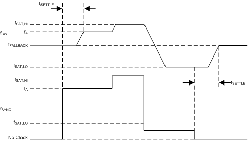
Figure 5-10 shows the frequency of SYNCDCDC input clock (fSYNC) and the frequency of PLL output signal (fSW).
 Figure 5-10 Synchronized Clock Frequency
 When no clock is present on the SYNCDCDC pin, the PLL generates a clock with a frequency equal to the fallback frequency (fFALLBACK).
When a clock is present on the SYNCDCDC pin with a frequency between the low and high PLL saturation frequencies (fSAT,LO and fSAT,HI), then the PLL is synchronized on the SYNCDCDC clock and generates a clock with frequency equal to fSYNC.
If fSYNC is higher than fSAT,HI, then the PLL generates a clock with a frequency equal to fSAT,HI.
If fSYNC is smaller than fSAT,LO, then the PLL generates a clock with a frequency equal to fSAT,LO.
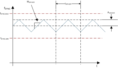
Dithering can be achieved by changing the frequency of the clock provided on the SYNCDCDC pin. The sync clock dither specification parameters are based on a triangular dither pattern, but other patterns that comply with the minimum and maximum sync frequency range and the maximum dither slope can also be used, as seen in Figure 5-11.
 Figure 5-11 Synchronized Clock Frequency Range and Dither