ZHCSFH6C March 2016 – February 2019 TPS65916
PRODUCTION DATA.
- 1器件概述
- 2修订历史记录
- 3Pin Configuration and Functions
-
4Specifications
- 4.1 Absolute Maximum Ratings
- 4.2 ESD Ratings
- 4.3 Recommended Operating Conditions
- 4.4 Thermal Information
- 4.5 Electrical Characteristics — LDO Regulators
- 4.6 Electrical Characteristics — SMPS1&2 in Dual-Phase Configuration
- 4.7 Electrical Characteristics — SMPS1, SMPS2, SMPS3, SMPS4, and SMPS5 Stand-Alone Regulators
- 4.8 Electrical Characteristics — Reference Generator (Bandgap)
- 4.9 Electrical Characteristics — 32-kHz RC Oscillators and SYNCCLKOUT Output Buffers
- 4.10 Electrical Characteristics — 12-Bit Sigma-Delta ADC
- 4.11 Electrical Characteristics — Thermal Monitoring and Shutdown
- 4.12 Electrical Characteristics — System Control Thresholds
- 4.13 Electrical Characteristics — Current Consumption
- 4.14 Electrical Characteristics — Digital Input Signal Parameters
- 4.15 Electrical Characteristics — Digital Output Signal Parameters
- 4.16 I/O Pullup and Pulldown Characteristics
- 4.17 Electrical Characteristics — I2C Interface
- 4.18 Timing Requirements — I2C Interface
- 4.19 Timing Requirements — SPI
- 4.20 Switching Characteristics — LDO Regulators
- 4.21 Switching Characteristics — SMPS1&2 in Dual-Phase Configuration
- 4.22 Switching Characteristics — SMPS1, SMPS2, SMPS3, SMPS4, and SMPS5 Stand-Alone Regulators
- 4.23 Switching Characteristics — Reference Generator (Bandgap)
- 4.24 Switching Characteristics — PLL for SMPS Clock Generation
- 4.25 Switching Characteristics — 32-kHz RC Oscillators and SYNCCLKOUT Output Buffers
- 4.26 Switching Characteristics — 12-Bit Sigma-Delta ADC
- 4.27 Typical Characteristics
-
5Detailed Description
- 5.1 Overview
- 5.2 Functional Block Diagram
- 5.3 Device State Machine
- 5.4
Power Resources (Step-Down and Step-Up SMPS Regulators, LDOs)
- 5.4.1 Step-Down Regulators
- 5.4.2 Low Dropout Regulators (LDOs)
- 5.5 SMPS and LDO Input Supply Connections
- 5.6 First Supply Detection
- 5.7 Long-Press Key Detection
- 5.8 12-Bit Sigma-Delta General-Purpose ADC (GPADC)
- 5.9 General-Purpose I/Os (GPIO Pins)
- 5.10 Thermal Monitoring
- 5.11 Interrupts
- 5.12 Control Interfaces
- 5.13 OTP Configuration Memory
- 5.14 Watchdog Timer (WDT)
- 5.15 System Voltage Monitoring
- 5.16 Register Map
- 5.17 Device Identification
- 6Applications, Implementation, and Layout
- 7器件和文档支持
- 8机械、封装和可订购信息
5.4.1.6 Step-Down Converters SMPS1, SMPS2 or SMPS1&2
The step-down converters, SMPS1 and SMPS2, can be used in two different configurations which are described as follows:
- SMPS1 and SMPS2 in single-phase configuration with each SMPS supporting a 3.5-A load current
- SMPS1&2 in dual-phase configuration supporting 7-A load current
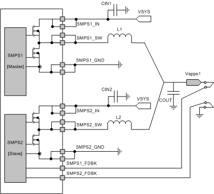
SMPS1 and SMPS2 can be used as separate converters. In dual-phase configuration the two interleaved synchronous buck-regulator phases with built-in current sharing operate in opposite phases. For light loads, the converter automatically changes to single-phase operation.
Figure 5-14 shows the connections for dual-phase configurations.
 Figure 5-14 SMPS1&2 Dual-Phase Configuration
 Below are the steps to program the SMPS1 and SMPS2 for single-phase or dual-phase operation:
- The OTP bit defines single-phase (SMPS1 and SMPS2) or dual-phase (SMPS1&2) operation. If dual-phase mode is selected, the SMPS12 registers control SMPS1&2.
- By default, SMPS1&2 operates in dual-phase mode for higher load currents and switches automatically to single-phase mode for low load currents. Forcing multiphase operation or single-phase operation is possible by setting the SMPS_CTRL.SMPS12_PHASE_CTRL[1:0] bits when the SMPS1&2 are loaded. Under no-load condition, do not force the multiphase operation because it causes SMPS12 to exhibit instability.