ZHCSFH6C March 2016 – February 2019 TPS65916
PRODUCTION DATA.
- 1器件概述
- 2修订历史记录
- 3Pin Configuration and Functions
-
4Specifications
- 4.1 Absolute Maximum Ratings
- 4.2 ESD Ratings
- 4.3 Recommended Operating Conditions
- 4.4 Thermal Information
- 4.5 Electrical Characteristics — LDO Regulators
- 4.6 Electrical Characteristics — SMPS1&2 in Dual-Phase Configuration
- 4.7 Electrical Characteristics — SMPS1, SMPS2, SMPS3, SMPS4, and SMPS5 Stand-Alone Regulators
- 4.8 Electrical Characteristics — Reference Generator (Bandgap)
- 4.9 Electrical Characteristics — 32-kHz RC Oscillators and SYNCCLKOUT Output Buffers
- 4.10 Electrical Characteristics — 12-Bit Sigma-Delta ADC
- 4.11 Electrical Characteristics — Thermal Monitoring and Shutdown
- 4.12 Electrical Characteristics — System Control Thresholds
- 4.13 Electrical Characteristics — Current Consumption
- 4.14 Electrical Characteristics — Digital Input Signal Parameters
- 4.15 Electrical Characteristics — Digital Output Signal Parameters
- 4.16 I/O Pullup and Pulldown Characteristics
- 4.17 Electrical Characteristics — I2C Interface
- 4.18 Timing Requirements — I2C Interface
- 4.19 Timing Requirements — SPI
- 4.20 Switching Characteristics — LDO Regulators
- 4.21 Switching Characteristics — SMPS1&2 in Dual-Phase Configuration
- 4.22 Switching Characteristics — SMPS1, SMPS2, SMPS3, SMPS4, and SMPS5 Stand-Alone Regulators
- 4.23 Switching Characteristics — Reference Generator (Bandgap)
- 4.24 Switching Characteristics — PLL for SMPS Clock Generation
- 4.25 Switching Characteristics — 32-kHz RC Oscillators and SYNCCLKOUT Output Buffers
- 4.26 Switching Characteristics — 12-Bit Sigma-Delta ADC
- 4.27 Typical Characteristics
-
5Detailed Description
- 5.1 Overview
- 5.2 Functional Block Diagram
- 5.3 Device State Machine
- 5.4
Power Resources (Step-Down and Step-Up SMPS Regulators, LDOs)
- 5.4.1 Step-Down Regulators
- 5.4.2 Low Dropout Regulators (LDOs)
- 5.5 SMPS and LDO Input Supply Connections
- 5.6 First Supply Detection
- 5.7 Long-Press Key Detection
- 5.8 12-Bit Sigma-Delta General-Purpose ADC (GPADC)
- 5.9 General-Purpose I/Os (GPIO Pins)
- 5.10 Thermal Monitoring
- 5.11 Interrupts
- 5.12 Control Interfaces
- 5.13 OTP Configuration Memory
- 5.14 Watchdog Timer (WDT)
- 5.15 System Voltage Monitoring
- 5.16 Register Map
- 5.17 Device Identification
- 6Applications, Implementation, and Layout
- 7器件和文档支持
- 8机械、封装和可订购信息
5.15 System Voltage Monitoring
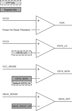
Comparators that monitor the voltage on the VCC_SENSE, and VCCA pins control the power state machine of the TPS65916 device. For electrical parameters, see Section 4.12.
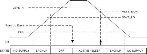
- PORWhen the supply at the VCCA pin is below the POR threshold, the TPS65916 device is in the NO SUPPLY state. All functionality is off. The device moves from the NO SUPPLY state to the BACKUP state when the voltage in VCCA rises above the POR threshold.
- VSYS_LOWhen the voltage on the VCCA pin rises above VSYS_LO, the device enters from the BACKUP state to the OFF state. When the device is in an ACTIVE, SLEEP, or OFF state and the voltage on VCCA decreases below the VSYS_LO level, the device enters backup mode. When the device transitions from the ACTIVE state to the BACKUP state, all active SMPS and LDO regulators, except LDOVRTC, are disabled simultaneously. There is a 180-µs deglitch time after VCCA becomes less than VSYS_LO and before the regulators are disabled. The level of VSYS_LO is OTP programmable.
- VSYS_MONDuring power up, the value of VSYS_HI OTP is used as a threshold for the VSYS_MON comparator which is gating PMIC start-up (that is, as a threshold for transition from the OFF state to the ACTIVE state). The VSYS_MON comparator monitors the VCC_SENSE pin. After power up, software can configure the comparator threshold in the VSYS_MON register.
- VBUS_DETThe VBUS_DET comparator is monitoring the VBUS_SENSE (secondary function of GPIO1) pin. This comparator is active when VCCA is greater than the POR threshold. Triggering the threshold level generates an interrupt. It can wake up the device from the SLEEP state, but can also switch on the device from the OFF state.
Figure 5-25 shows a block diagram of the system comparators and Figure 5-26 shows the state transitions.
 Figure 5-25 System Comparators
  Figure 5-26 State Transitions
 NOTE
To generate a POR from a falling VCC, VCC is sampled every 1 ms and compared to the POR threshold. In case VCC is discharged and resupplied quickly, a POR may not be reliably generated if VCC crosses the POR threshold between samples. Another way to generate POR is to discharge the LDOVRTC regulator to 0 V after VCC is removed. With no external load, this could take seconds for the LDOVRTC output to discharge to 0 V. The PMIC should not be restarted after VCC is removed but before LDOVRTC is discharged to 0 V. If necessary, TI recommends adding a pulldown resistor from the LDOVRTC output to GND with a minimum of 3.9 kΩ to speed up the LDOVRTC discharge time.
The value of the pulldown resistor should be chosen based on the desired discharge time and acceptable current draw in the OFF state, but no greater than 0.5 mA. Use Equation 7 to calculate the pulldown resistor based on the desired discharge time.

where
- tdischarge = discharge time of the VRTC output
- RPD = pulldown resistance from the VRTC output to GND
- CO = output capacitance on the VRTC line (typically 2.2 µF)
Because LDOVRTC is always on when VCC is supplied, additional current is drawn through the pulldown resistor. The output current of LDOVRTC while the PMIC is in OFF state should not exceed 0.5 mA. Use Equation 8 to calculate the pulldown current.

where
- IPD = current through the pulldown resistor
- RPD = pulldown resistance from the VRTC regulator
To use comparators in the system:
- The VSYS_HI and VSYS_LO thresholds are defined in the OTP. Software cannot change these levels.
- After startup, the VSYS_MON comparator is automatically disabled. Software can select new threshold levels using the VSYS_MON register and then enable the comparators.
- To have the same coding for rising and falling edge, the VSYS_MON comparator does not include hysteresis and thus can generate multiple interrupts when the voltage level is at threshold level. New interrupt generation has a 125-µs debounce time. This time lets software mask the interrupt and update the threshold level or disable the comparator before receiving a new interrupt.
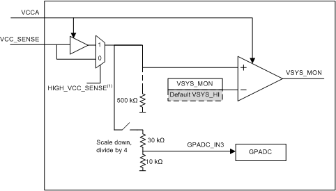
Figure 5-27 shows more details on VSYS_MON comparator. When the VSYS_MON comparator is enabled, and the internal buffer is bypassed, the input impedance at VCC_SENSE pin is 500 kΩ (typical). When the comparator is disabled, the VCC_SENSE pin is in the high-impedance state. If GPADC is enabled to measure channel 2 or channel 3, 40 kΩ is added in parallel to the corresponding comparator. See Table 5-9 for GPADC input range.
To enable system voltage sensing above 5.25 V, an external resistive divider can be used. Internal buffers can be enabled by setting the OTP bit HIGH_VCC_SENSE to 1 to provide high impedance for the external resistive dividers. The maximum input level for the internal buffer is VCCA – 1 V.
