ZHCSGJ3D July 2015 – February 2019 TPS65917-Q1
PRODUCTION DATA.
- 1器件概述
- 2修订历史记录
- 3Pin Configuration and Functions
-
4Specifications
- 4.1 Absolute Maximum Ratings
- 4.2 ESD Ratings
- 4.3 Recommended Operating Conditions
- 4.4 Thermal Information
- 4.5 Electrical Characteristics — LDO Regulators
- 4.6 Electrical Characteristics — SMPS1&2 in Dual-Phase Configuration
- 4.7 Electrical Characteristics — SMPS1, SMPS2, SMPS3, SMPS4, and SMPS5 Stand-Alone Regulators
- 4.8 Electrical Characteristics — Reference Generator (Bandgap)
- 4.9 Electrical Characteristics — 32-kHz RC Oscillators and SYNCCLKOUT Output Buffers
- 4.10 Electrical Characteristics — 12-Bit Sigma-Delta ADC
- 4.11 Electrical Characteristics — Thermal Monitoring and Shutdown
- 4.12 Electrical Characteristics — System Control Thresholds
- 4.13 Electrical Characteristics — Current Consumption
- 4.14 Electrical Characteristics — Digital Input Signal Parameters
- 4.15 Electrical Characteristics — Digital Output Signal Parameters
- 4.16 I/O Pullup and Pulldown Characteristics
- 4.17 Electrical Characteristics — I2C Interface
- 4.18 Timing Requirements — I2C Interface
- 4.19 Timing Requirements — SPI
- 4.20 Switching Characteristics — LDO Regulators
- 4.21 Switching Characteristics — SMPS1&2 in Dual-Phase Configuration
- 4.22 Switching Characteristics — SMPS1, SMPS2, SMPS3, SMPS4, and SMPS5 Stand-Alone Regulators
- 4.23 Switching Characteristics — Reference Generator (Bandgap)
- 4.24 Switching Characteristics — PLL for SMPS Clock Generation
- 4.25 Switching Characteristics — 32-kHz RC Oscillators and SYNCCLKOUT Output Buffers
- 4.26 Switching Characteristics — 12-Bit Sigma-Delta ADC
- 4.27 Typical Characteristics
-
5Detailed Description
- 5.1 Overview
- 5.2 Functional Block Diagram
- 5.3 Device State Machine
- 5.4
Power Resources (Step-Down and Step-Up SMPS Regulators, LDOs)
- 5.4.1 Step-Down Regulators
- 5.4.2 Low Dropout Regulators (LDOs)
- 5.5 SMPS and LDO Input Supply Connections
- 5.6 First Supply Detection
- 5.7 Long-Press Key Detection
- 5.8 12-Bit Sigma-Delta General-Purpose ADC (GPADC)
- 5.9 General-Purpose I/Os (GPIO Pins)
- 5.10 Thermal Monitoring
- 5.11 Interrupts
- 5.12 Control Interfaces
- 5.13 OTP Configuration Memory
- 5.14 Watchdog Timer (WDT)
- 5.15 System Voltage Monitoring
- 5.16 Register Map
- 5.17 Device Identification
- 6Applications, Implementation, and Layout
- 7器件和文档支持
- 8机械、封装和可订购信息
5.3.7 Reset Levels
The TPS65917-Q1 resource control registers are defined by the following three categories:
- Power-on request (POR) registers
- Hardware (HW) registers
- Switchoff (SWO) registers
These registers are associated to three levels of reset which are described as follows
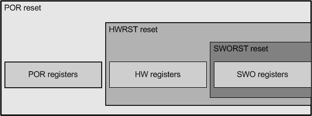
- Power-on reset (POR) A POR occurs when the device receives supplies and transition from the NO SUPPLY state to the BACKUP state. The POR is the global device reset which resets all registers.
- SMPS_THERMAL_STATUS
- SMPS_SHORT_STATUS
- SMPS_POWERGOOD_MASK
- LDO_SHORT_STATUS
- SWOFF_STATUS
The values of the registers in this domain will retain their value under HWRST and SWORST event. This ensures the information which contains the cause of the switch off event is retained when the device is reset to its default operating state.
The following registers are reset only during POR event:
This list is indicative only; a full list and bit details can be found in the TPS65917-Q1 Register Map (SLVUAH1).
- Hardware reset (HWRST) A HWRST occurs when any OFF request is configured to generate a hardware reset. Configuration of the reset level is programmed in the SWOFF_HWRST register. This reset triggers a transition to the OFF state from either the ACTIVE or SLEEP state, and therefore executes the ACT2OFF or SLP2OFF sequence.
- SMPS control registers expect MODE_ACTIVE and MODE_SLEEP bits
- LDO control registers expect MODE_ACTIVE and MODE_SLEEP bits
- VSYS_LO Threshold
- PMU_CONFIG & PMU_CTRL
- NSLEEP, ENABLE1, and ENABLE2 resource assignment registers
- Input and Output, including the GPIO pins, Configuration and Control registers
- Interrupt Control, Status and Mask Registers
- OTP CRC results register
- GPADC Configuration and Results registers
A HWRST will reset all registers in the HWRST and the SWORST domain, but leave the registers in the POR domain unchanged.
The following registers are in the HWRST domain:
This list is indicative only; a full list and bit details can be found in the TPS65917-Q1 Register Map (SLVUAH1).
- Switch-off reset (SWORST) A SWORST occurs when any OFF request is configured to not generate a hardware reset. Configuration is done in the SWOFF_HWRST register. This reset acts like the HWRST, except only the SWO registers are reset. The TPS65917-Q1 goes into the OFF state, from either ACTIVE or SLEEP, and therefore executes the ACT2OFF or SLP2OFF sequence.
- SMPS control registers for voltage levels and operating mode control
- LDO control registers for voltage levels and operating mode control
- DEV_CTRL & POWER_CTRL registers
- VSYS_MON enable and result register
- WATCHDOG configuration register
- PLL and REGEN Control registers
A SWORST only resets registers in the SWORST domain, but leave the registers in the HWRST and POR domains unchanged.
The following registers are in the SWORST domain:
This list is indicative only; a full list and bit details can be found in the TPS65917-Q1 Register Map (SLVUAH1).
Table 5-7 lists the reset levels, and Figure 5-9 shows the reset levels versus registers.
Table 5-7 Reset Levels
| LEVEL | RESET TAG | REGISTERS AFFECTED | COMMENT |
|---|---|---|---|
| 0 | POR | POR, HW, SWO | This reset level is the lowest level, for which all registers are reset. |
| 1 | HWRST | HW, SWO | During hardware reset (HWRST), all registers are reset except the POR registers. |
| 2 | SWORST | SWO | Only the SWO registers are reset. |
 Figure 5-9 Reset Levels versus Registers