ZHCSGS5A August 2017 – February 2019 TPS65919-Q1
PRODUCTION DATA.
- 1器件概述
- 2修订历史记录
- 3Pin Configuration and Functions
-
4Specifications
- 4.1 Absolute Maximum Ratings
- 4.2 ESD Ratings
- 4.3 Recommended Operating Conditions
- 4.4 Thermal Information
- 4.5 Electrical Characteristics — LDO Regulators
- 4.6 Electrical Characteristics — SMPS1&2 in Dual-Phase Configuration
- 4.7 Electrical Characteristics — SMPS1, SMPS2, SMPS3, and SMPS4 Stand-Alone Regulators
- 4.8 Electrical Characteristics — Reference Generator (Bandgap)
- 4.9 Electrical Characteristics — 32-kHz RC Oscillators and SYNCCLKOUT Output Buffers
- 4.10 Electrical Characteristics — 12-Bit Sigma-Delta ADC
- 4.11 Electrical Characteristics — Thermal Monitoring and Shutdown
- 4.12 Electrical Characteristics — System Control Thresholds
- 4.13 Electrical Characteristics — Current Consumption
- 4.14 Electrical Characteristics — Digital Input Signal Parameters
- 4.15 Electrical Characteristics — Digital Output Signal Parameters
- 4.16 I/O Pullup and Pulldown Characteristics
- 4.17 Electrical Characteristics — I2C Interface
- 4.18 Timing Requirements — I2C Interface
- 4.19 Timing Requirements — SPI
- 4.20 Switching Characteristics — LDO Regulators
- 4.21 Switching Characteristics — SMPS1&2 in Dual-Phase Configuration
- 4.22 Switching Characteristics — SMPS1, SMPS2, SMPS3, and SMPS4 Stand-Alone Regulators
- 4.23 Switching Characteristics — Reference Generator (Bandgap)
- 4.24 Switching Characteristics — PLL for SMPS Clock Generation
- 4.25 Switching Characteristics — 32-kHz RC Oscillators and SYNCCLKOUT Output Buffers
- 4.26 Switching Characteristics — 12-Bit Sigma-Delta ADC
- 4.27 Typical Characteristics
-
5Detailed Description
- 5.1 Overview
- 5.2 Functional Block Diagram
- 5.3 Device State Machine
- 5.4
Power Resources (Step-Down and Step-Up SMPS Regulators, LDOs)
- 5.4.1 Step-Down Regulators
- 5.4.2 Low Dropout Regulators (LDOs)
- 5.5 SMPS and LDO Input Supply Connections
- 5.6 First Supply Detection
- 5.7 Long-Press Key Detection
- 5.8 12-Bit Sigma-Delta General-Purpose ADC (GPADC)
- 5.9 General-Purpose I/Os (GPIO Pins)
- 5.10 Thermal Monitoring
- 5.11 Interrupts
- 5.12 Control Interfaces
- 5.13 OTP Configuration Memory
- 5.14 Watchdog Timer (WDT)
- 5.15 System Voltage Monitoring
- 5.16 Register Map
- 5.17 Device Identification
- 6Applications, Implementation, and Layout
- 7器件和文档支持
- 8机械、封装和可订购信息
5.4.1.5 DVS-Capable Regulators
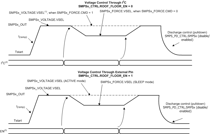
The Step-down converters, SMPS1, SMPS2, or SMPS1&2 and SMPS3, are DVS-capable and have some additional parameters for control. The slew rate of the output voltage during a voltage level change is fixed at 2.5 mV/μs. The control for two different voltage levels (roof and floor) with the NSLEEP, ENABLE1, and ENABLE2 signals is available. When the roof-floor control is not used (ROOF_FLOOR_EN = 0), the CMD bit in the SMPSx_FORCE register can select two different voltage levels.
Below are the steps for programming two difference output voltage levels (roof and floor) for the DVS-capable step-down converters:
- The NSLEEP, ENABLE1, or ENABLE2 pins can be used for roof-floor control of SMPS. For roof-floor operation, set the SMPSx_CTRL.ROOF_FLOOR_EN register, and assign SMPS to NSLEEP, ENABLE1, and ENABLE2 in the NSLEEP_SMPS_ASSIGN, ENABLE1_SMPS_ASSIGN, and ENABLE2_SMPS_ASSIGN registers, respectively. When the controlling pin is active, the value for the SMPS output is defined by the SMPSx_VOLTAGE register. When the controlling pin is not active, the value for the SMPS output is defined by the SMPSx_FORCE register.
- Set the second value for the output voltage with the SMPSx_FORCE.VSEL register. Setting this register to 0x0 turns off the SMPS.
- Select which register, SMPSx_VOLTAGE or SMPSx_FORCE, to use with the SMPSx_FORCE.CMD bit. The default is the voltage setting of SMPSx_VOLTAGE. For the CMD bit to work, ensure that the SMPSx_CTRL.ROOF_FLOOR_EN bit is set to 0.
Figure 5-13 shows the SMPS controls for DVS.

1. VSEL[6:0] (voltage selection):
SMPSx_VOLTAGE.RANGE = 0: OFF, 0.5 V to 1.65 V in 10-mV steps
SMPSx_VOLTAGE.RANGE = 1: 1 to 3.3 V in 20-mV steps
SMPSx_VOLTAGE.RANGE = 0: OFF, 0.5 V to 1.65 V in 10-mV steps
SMPSx_VOLTAGE.RANGE = 1: 1 to 3.3 V in 20-mV steps
2. I2C: Control through access to SMPSx_VOLTAGE, SMPSx_FORCE registers
3. EN: Control through NSLEEP, ENABLE1, and ENABLE2 pins (see Table 5-5)
Figure 5-13 SMPS Controls for DVS