ZHCSKK3B December   2019  – February 2022 TPS6594-Q1

PRODUCTION DATA  

  1. 特性
  2. 应用
  3. 说明
    1.     4
  4. Revision History
  5. 说明(续)
  6. Pin Configuration and Functions
    1. 6.1 Digital Signal Descriptions
  7. Specifications
    1. 7.1  Absolute Maximum Ratings
    2. 7.2  ESD Ratings
    3. 7.3  Recommended Operating Conditions
    4. 7.4  Thermal Information
    5. 7.5  General Purpose Low Drop-Out Regulators (LDO1, LDO2, LDO3)
    6. 7.6  Low Noise Low Drop-Out Regulator (LDO4)
    7. 7.7  Internal Low Drop-Out Regulators (LDOVRTC, LDOVINT)
    8. 7.8  BUCK1, BUCK2, BUCK3, BUCK4 and BUCK5 Regulators
    9. 7.9  Reference Generator (BandGap)
    10. 7.10 Monitoring Functions
    11. 7.11 Clocks, Oscillators, and PLL
    12. 7.12 Thermal Monitoring and Shutdown
    13. 7.13 System Control Thresholds
    14. 7.14 Current Consumption
    15. 7.15 Backup Battery Charger
    16. 7.16 Digital Input Signal Parameters
    17. 7.17 Digital Output Signal Parameters
    18. 7.18 I/O Pullup and Pulldown Resistance
    19. 7.19 I2C Interface
    20. 7.20 Serial Peripheral Interface (SPI)
    21. 7.21 Typical Characteristics
  8. Detailed Description
    1. 8.1 Overview
    2. 8.2 Functional Block Diagram
    3. 8.3 Feature Description
      1. 8.3.1  System Supply Voltage Monitor and Over-Voltage Protection
      2. 8.3.2  Power Resources (Bucks and LDOs)
        1. 8.3.2.1 Buck Regulators
          1. 8.3.2.1.1  BUCK Regulator Overview
          2. 8.3.2.1.2  Multi-Phase Operation and Phase-Adding or Shedding
          3. 8.3.2.1.3  Transition Between PWM and PFM Modes
          4. 8.3.2.1.4  Multi-Phase BUCK Regulator Configurations
          5. 8.3.2.1.5  Spread-Spectrum Mode
          6. 8.3.2.1.6  Adaptive Voltage Scaling (AVS) and Dynamic Voltage Scaling (DVS) Support
          7. 8.3.2.1.7  BUCK Output Voltage Setting
          8. 8.3.2.1.8  BUCK Regulator Current Limit
          9. 8.3.2.1.9  SW_Bx Short-to-Ground Detection
          10. 8.3.2.1.10 Sync Clock Functionality
          11.        48
        2. 8.3.2.2 Low Dropout Regulators (LDOs)
          1. 8.3.2.2.1 LDOVINT
          2. 8.3.2.2.2 LDOVRTC
          3. 8.3.2.2.3 LDO1, LDO2, and LDO3
          4. 8.3.2.2.4 Low-Noise LDO (LDO4)
      3. 8.3.3  Residual Voltage Checking
      4. 8.3.4  Output Voltage Monitor and PGOOD Generation
      5. 8.3.5  Thermal Monitoring
        1. 8.3.5.1 Thermal Warning Function
        2. 8.3.5.2 Thermal Shutdown
      6. 8.3.6  Backup Supply Power-Path
      7. 8.3.7  General-Purpose I/Os (GPIO Pins)
      8. 8.3.8  nINT, EN_DRV, and nRSTOUT Pins
      9. 8.3.9  Interrupts
      10. 8.3.10 RTC
        1. 8.3.10.1 General Description
        2. 8.3.10.2 Time Calendar Registers
          1. 8.3.10.2.1 TC Registers Read Access
          2. 8.3.10.2.2 TC Registers Write Access
        3. 8.3.10.3 RTC Alarm
        4. 8.3.10.4 RTC Interrupts
        5. 8.3.10.5 RTC 32-kHz Oscillator Drift Compensation
      11. 8.3.11 Watchdog (WDOG)
        1. 8.3.11.1 Watchdog Fail Counter and Status
        2. 8.3.11.2 Watchdog Start-Up and Configuration
        3. 8.3.11.3 MCU to Watchdog Synchronization
        4. 8.3.11.4 Watchdog Disable Function
        5. 8.3.11.5 Watchdog Sequence
        6. 8.3.11.6 Watchdog Trigger Mode
        7. 8.3.11.7 WatchDog Flow Chart and Timing Diagrams in Trigger Mode
        8.       79
        9. 8.3.11.8 Watchdog Question-Answer Mode
          1. 8.3.11.8.1 Watchdog Q&A Related Definitions
          2. 8.3.11.8.2 Question Generation
          3. 8.3.11.8.3 Answer Comparison
            1. 8.3.11.8.3.1 Sequence of the 2-bit Watchdog Answer Counter
            2. 8.3.11.8.3.2 Watchdog Sequence Events and Status Updates
            3. 8.3.11.8.3.3 Watchdog Q&A Sequence Scenarios
      12. 8.3.12 Error Signal Monitor (ESM)
        1. 8.3.12.1 ESM Error-Handling Procedure
          1. 8.3.12.1.1 Level Mode
          2.        90
          3. 8.3.12.1.2 PWM Mode
            1. 8.3.12.1.2.1 Good-Events and Bad-Events
            2. 8.3.12.1.2.2 ESM Error-Counter
            3. 8.3.12.1.2.3 ESM Start-Up in PWM Mode
            4. 8.3.12.1.2.4 ESM Flow Chart and Timing Diagrams in PWM Mode
            5.         96
    4. 8.4 Device Functional Modes
      1. 8.4.1 Device State Machine
        1. 8.4.1.1 Fixed Device Power FSM
          1. 8.4.1.1.1 Register Resets and NVM Read at INIT State
        2. 8.4.1.2 Pre-Configurable Mission States
          1. 8.4.1.2.1 PFSM Commands
            1. 8.4.1.2.1.1  REG_WRITE_IMM Command
            2. 8.4.1.2.1.2  REG_WRITE_MASK_IMM Command
            3. 8.4.1.2.1.3  REG_WRITE_MASK_PAGE0_IMM Command
            4. 8.4.1.2.1.4  REG_WRITE_BIT_PAGE0_IMM Command
            5. 8.4.1.2.1.5  REG_WRITE_WIN_PAGE0_IMM Command
            6. 8.4.1.2.1.6  REG_WRITE_VOUT_IMM Command
            7. 8.4.1.2.1.7  REG_WRITE_VCTRL_IMM Command
            8. 8.4.1.2.1.8  REG_WRITE_MASK_SREG Command
            9. 8.4.1.2.1.9  SREG_READ_REG Command
            10. 8.4.1.2.1.10 SREG_WRITE_IMM Command
            11. 8.4.1.2.1.11 WAIT Command
            12. 8.4.1.2.1.12 DELAY_IMM Command
            13. 8.4.1.2.1.13 DELAY_SREG Command
            14. 8.4.1.2.1.14 TRIG_SET Command
            15. 8.4.1.2.1.15 TRIG_MASK Command
            16. 8.4.1.2.1.16 END Command
          2. 8.4.1.2.2 Configuration Memory Organization and Sequence Execution
          3. 8.4.1.2.3 Mission State Configuration
          4. 8.4.1.2.4 Pre-Configured Hardware Transitions
            1. 8.4.1.2.4.1 ON Requests
            2. 8.4.1.2.4.2 OFF Requests
            3. 8.4.1.2.4.3 NSLEEP1 and NSLEEP2 Functions
            4. 8.4.1.2.4.4 WKUP1 and WKUP2 Functions
            5. 8.4.1.2.4.5 LP_WKUP Pins for Waking Up from LP STANDBY
        3. 8.4.1.3 Error Handling Operations
          1. 8.4.1.3.1 Power Rail Output Error
          2. 8.4.1.3.2 Boot BIST Error
          3. 8.4.1.3.3 Runtime BIST Error
          4. 8.4.1.3.4 Catastrophic Error
          5. 8.4.1.3.5 Watchdog (WDOG) Error
          6. 8.4.1.3.6 Error Signal Monitor (ESM) Error
          7. 8.4.1.3.7 Warnings
        4. 8.4.1.4 Device Start-up Timing
        5. 8.4.1.5 Power Sequences
        6. 8.4.1.6 First Supply Detection
        7. 8.4.1.7 Register Power Domains and Reset Levels
      2. 8.4.2 Multi-PMIC Synchronization
        1. 8.4.2.1 SPMI Interface System Setup
        2. 8.4.2.2 Transmission Protocol and CRC
          1. 8.4.2.2.1 Operation with Transmission Errors
          2. 8.4.2.2.2 Transmitted Information
        3. 8.4.2.3 SPMI Target Device Communication to SPMI Controller Device
          1. 8.4.2.3.1 Incomplete Communication from SPMI Target Device to SPMI Controller Device
        4. 8.4.2.4 SPMI-BIST Overview
          1. 8.4.2.4.1 SPMI Bus during Boot BIST and RUNTIME BIST
          2. 8.4.2.4.2 Periodic Checking of the SPMI
          3. 8.4.2.4.3 SPMI Message Priorities
    5. 8.5 Control Interfaces
      1. 8.5.1 CRC Calculation for I2C and SPI Interface Protocols
      2. 8.5.2 I2C-Compatible Interface
        1. 8.5.2.1 Data Validity
        2. 8.5.2.2 Start and Stop Conditions
        3. 8.5.2.3 Transferring Data
        4. 8.5.2.4 Auto-Increment Feature
      3. 8.5.3 Serial Peripheral Interface (SPI)
    6. 8.6 Configurable Registers
      1. 8.6.1 Register Page Partitioning
      2. 8.6.2 CRC Protection for Configuration, Control, and Test Registers
      3. 8.6.3 CRC Protection for User Registers
      4. 8.6.4 Register Write Protection
        1. 8.6.4.1 ESM and WDOG Configuration Registers
        2. 8.6.4.2 User Registers
    7. 8.7 Register Maps
      1. 8.7.1 TPS6594-Q1 Registers
  9. Application and Implementation
    1. 9.1 Application Information
    2. 9.2 Typical Application
      1. 9.2.1 Powering a Processor
        1. 9.2.1.1 Design Requirements
        2. 9.2.1.2 Detailed Design Procedure
          1. 9.2.1.2.1 VCCA, VSYS_SENSE, and OVPGDRV
          2. 9.2.1.2.2 Internal LDOs
          3. 9.2.1.2.3 Crystal Oscillator
          4. 9.2.1.2.4 Buck Input Capacitors
          5. 9.2.1.2.5 Buck Output Capacitors
          6. 9.2.1.2.6 Buck Inductors
          7. 9.2.1.2.7 LDO Input Capacitors
          8. 9.2.1.2.8 LDO Output Capacitors
          9. 9.2.1.2.9 Digital Signal Connections
      2. 9.2.2 Application Curves
  10. 10Power Supply Recommendations
  11. 11Layout
    1. 11.1 Layout Guidelines
    2. 11.2 Layout Example
  12. 12Device and Documentation Support
    1. 12.1 Device Support
      1. 12.1.1 第三方米6体育平台手机版_好二三四免责声明
    2. 12.2 Device Nomenclature
    3. 12.3 Documentation Support
    4. 12.4 Receiving Notification of Documentation Updates
    5. 12.5 支持资源
    6. 12.6 Trademarks
    7. 12.7 Electrostatic Discharge Caution
    8. 12.8 术语表
  13. 13Mechanical, Packaging, and Orderable Information

封装选项

机械数据 (封装 | 引脚)
散热焊盘机械数据 (封装 | 引脚)
订购信息

Device Start-up Timing

Figure 8-44 shows the timing diagram of the TPS6594-Q1 after the first supply detection.
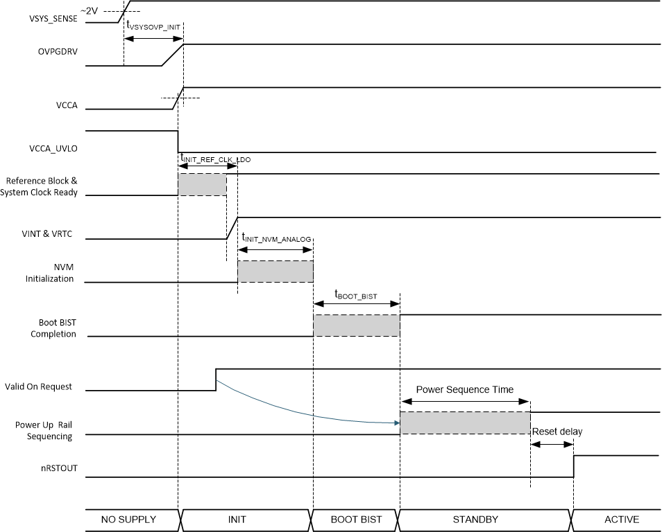
GUID-8ADFC5B2-6D83-4124-818E-F196C7F5D1AA-low.gif Figure 8-44 Device Start-up Timing Diagram

tVSYSOVP_INIT is the time between VSYS detection and when the VSYS Over Voltage Protection Module is in operation and the external protection FET connects the VSYS_SENSE to VCCA and the PVINx pins.

tINIT_REFCLK_LDO is the start-up time for the reference block. tINIT_NVM_ANALOG is the time for the device to load the default values of the NVM configurable registers from the NVM memory, and the start-up time for the analog circuits in the device. tINIT_REFCLK_LDO and tINIT_NVM_ANALOG are defined in the electrical characteristics table.

tBOOT_BIST is the sum of tABISTrun and tLBISTrun, which are defined in the electrical characterization tables.

The Power Sequence time is the total time for the device to complete the power up sequence. Please refer to Section 8.4.1.5 for more details.

The reset delay time is a configurable wait time for the nRSTOUT and the nRSTOUT_SoC release after the power up sequence is completed.