ZHCSFF4C February 2016 – August 2021 TPS65981
PRODUCTION DATA
- 1 特性
- 2 应用
- 3 说明
- 4 Revision History
- 5 说明(续)
- 6 Pin Configuration and Functions
-
7 Specifications
- 7.1 Absolute Maximum Ratings
- 7.2 ESD Ratings
- 7.3 Recommended Operating Conditions
- 7.4 Thermal Information
- 7.5 Power Supply Requirements and Characteristics
- 7.6 Power Supervisor Characteristics
- 7.7 Power Consumption Characteristics
- 7.8 Cable Detection Characteristics
- 7.9 USB-PD Baseband Signal Requirements and Characteristics
- 7.10 USB-PD TX Driver Voltage Adjustment Parameter
- 7.11 Port Power Switch Characteristics
- 7.12 Port Data Multiplexer Switching Characteristics
- 7.13 Port Data Multiplexer Clamp Characteristics
- 7.14 Port Data Multiplexer SBU Detection Requirements
- 7.15 Port Data Multiplexer Signal Monitoring Pullup and Pulldown Characteristics
- 7.16 Port Data Multiplexer USB Endpoint Requirements and Characteristics
- 7.17 Port Data Multiplexer BC1.2 Detection Requirements and Characteristics
- 7.18 Analog-to-Digital Converter (ADC) Characteristics
- 7.19 Input-Output (I/O) Requirements and Characteristics
- 7.20 I2C Slave Requirements and Characteristics
- 7.21 SPI Controller Characteristics
- 7.22 BUSPOWERZ Configuration Requirements
- 7.23 Single-Wire Debugger (SWD) Timing Requirements
- 7.24 Thermal Shutdown Characteristics
- 7.25 HPD Timing Requirements and Characteristics
- 7.26 Oscillator Requirements and Characteristics
- 7.27 Typical Characteristics
- 8 Parameter Measurement Information
-
9 Detailed Description
- 9.1 Overview
- 9.2 Functional Block Diagram
- 9.3
Feature Description
- 9.3.1 USB-PD Physical Layer
- 9.3.2 Cable Plug and Orientation Detection
- 9.3.3
Port Power Switches
- 9.3.3.1 5-V Power Delivery
- 9.3.3.2 5V Power Switch as a Source
- 9.3.3.3 PP_5V0 Current Sense
- 9.3.3.4 PP_5V0 Current Limit
- 9.3.3.5 Internal HV Power Delivery
- 9.3.3.6 Internal HV Power Switch as a Source
- 9.3.3.7 Internal HV Power Switch as a Sink
- 9.3.3.8 Internal HV Power Switch Current Sense
- 9.3.3.9 Internal HV Power Switch Current Limit
- 9.3.3.10 External HV Power Delivery
- 9.3.3.11 External HV Power Switch as a Source with RSENSE
- 9.3.3.12 External HV Power Switch as a Sink With RSENSE
- 9.3.3.13 External HV Power Switch as a Sink Without RSENSE
- 9.3.3.14 External Current Sense
- 9.3.3.15 External Current Limit
- 9.3.3.16 Soft Start
- 9.3.3.17 BUSPOWERZ
- 9.3.3.18 Voltage Transitions on VBUS through Port Power Switches
- 9.3.3.19 HV Transition to PP_RV0 Pull-down on VBUS
- 9.3.3.20 VBUS Transition to VSAFE0V
- 9.3.3.21 C_CC1 and C_CC2 Power Configuration and Power Delivery
- 9.3.3.22 PP_CABLE to C_CC1 and C_CC2 Switch Architecture
- 9.3.3.23 PP_CABLE to C_CC1 and C_CC2 Current Limit
- 9.3.4
USB Type-C® Port Data Multiplexer
- 9.3.4.1 USB Top and Bottom Ports
- 9.3.4.2 Multiplexer Connection Orientation
- 9.3.4.3 SBU Crossbar Multiplexer
- 9.3.4.4 Signal Monitoring and Pull-up and Pull-down
- 9.3.4.5 Port Multiplexer Clamp
- 9.3.4.6 USB2.0 Low-Speed Endpoint
- 9.3.4.7 Battery Charger (BC1.2) Detection Block
- 9.3.4.8 BC1.2 Data Contact Detect
- 9.3.4.9 BC1.2 Primary and Secondary Detection
- 9.3.5 Power Management
- 9.3.6 Digital Core
- 9.3.7 USB-PD BMC Modem Interface
- 9.3.8 System Glue Logic
- 9.3.9 Power Reset Congrol Module (PRCM)
- 9.3.10 Interrupt Monitor
- 9.3.11 ADC Sense
- 9.3.12 I2C Slave
- 9.3.13 SPI Controller
- 9.3.14 Single-Wire Debugger Interface
- 9.3.15 DisplayPort HPD Timers
- 9.3.16 ADC
- 9.3.17 I/O Buffers
- 9.3.18 Thermal Shutdown
- 9.3.19 Oscillators
- 9.4 Device Functional Modes
- 9.5 Programming
-
10Application and Implementation
- 10.1 Application Information
- 10.2
Typical Applications
- 10.2.1
Fully-Featured USB Type-C® and PD Charger
Application
- 10.2.1.1 Design Requirements
- 10.2.1.2
Detailed Design Procedure
- 10.2.1.2.1 TPS65981 External Flash
- 10.2.1.2.2 Debug Control (DEBUG_CTL) and I2C (I2C) Resistors
- 10.2.1.2.3 Oscillator (R_OSC) Resistor
- 10.2.1.2.4 VBUS Capacitor and Ferrite Bead
- 10.2.1.2.5 Soft Start (SS) Capacitor
- 10.2.1.2.6 USB Top (C_USB_T), USB Bottom (C_USB_B), and Sideband-Use (SBU) Connections
- 10.2.1.2.7 Port Power Switch (PP_EXT, PP_HV, PP_5V0, and PP_CABLE) Capacitors
- 10.2.1.2.8 Cable Connection (CCn) Capacitors and RPD_Gn Connections
- 10.2.1.2.9 LDO_3V3, LDO_1V8A, LDO_1V8D, LDO_BMC, VIN_3V3, and VDDIO
- 10.2.1.3 Application Curve
- 10.2.2
USB Type-C® and PD Dock or Monitor
Application
- 10.2.2.1 Design Requirements
- 10.2.2.2
Detailed Design Procedure
- 10.2.2.2.1 Port Power Switch (PP_5V0 and PP_CABLE) Capacitors
- 10.2.2.2.2 HD3SS460 Control and DisplayPort Configuration
- 10.2.2.2.3 AC-DC Power Supply (Barrel Jack) Detection Circuitry
- 10.2.2.2.4 TPS65981 Control of Variable Buck Regulator Output Voltage (PP_HV)
- 10.2.2.2.5 TPS65981 and System Controller Interaction
- 10.2.2.3 Application Curves
- 10.2.1
Fully-Featured USB Type-C® and PD Charger
Application
- 11Power Supply Recommendations
-
12Layout
- 12.1
Layout Guidelines
- 12.1.1 TPS65981 Recommended Footprint
- 12.1.2 Top TPS65981 Placement and Bottom Component Placement and Layout
- 12.1.3 Component Placement
- 12.1.4 Designs Rules and Guidance
- 12.1.5 Routing PP_HV, PP_EXT, PP_5V0, and VBUS
- 12.1.6 Routing Top and Bottom Passive Components
- 12.1.7 Thermal Pad Via Placement
- 12.1.8 Top Layer Routing
- 12.1.9 Inner Signal Layer Routing
- 12.1.10 Bottom Layer Routing
- 12.2 Layout Example
- 12.1
Layout Guidelines
- 13Device and Documentation Support
- 14Mechanical, Packaging, and Orderable Information
10.2.2.2.3 AC-DC Power Supply (Barrel Jack) Detection Circuitry
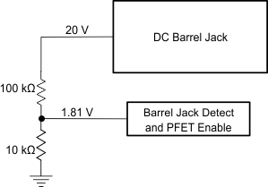
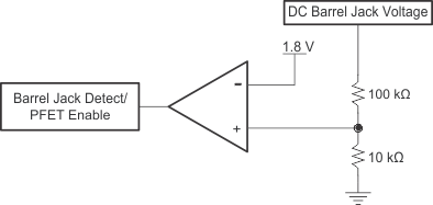
The system is design to either operate bus-powered over Type-C/PD or line-powered from the DC barrel jack. The TPS65981 detects that the DC barrel jack is connected to GPIOn. In the simplest form, a voltage divider could be set to the GPIO I/O level when the DC Barrel jack voltage is present, as shown in Figure 10-4. A comparator circuit is recommend and used in this design for design robustness, as shown in Figure 10-5. Figure 10-3 shows the barrel jack detection circuitry used in the dock or monitor application connected to GPIO2 configured as an input.
 Figure 10-4 DC Barrel Jack Voltage Divider
 Figure 10-5 Barrel Jack Detect Comparator
This detect signal is used to determine if the barrel jack is present to support the 20 V PD power contracts and to hand-off charging from barrel jack to Type-C or Type-C to barrel jack. When the DC barrel jack is detected the TPS65981 at the Type-C port will not request power as a USB PD sink and the system will be able to support a 5-20 V source power contract to another device. When the DC Barrel Jack is disconnected the TPS65981 will exit any 20 V source power contract and re-negotiate a power contract as a sink. When the DC Barrel Jack is re-connected the TPS65981 will send updated source capabilities and re-negotiate a power contract if possible.