ZHCSI93D May   2018  – October 2022 TPS65987D

PRODUCTION DATA  

  1. 特性
  2. 应用
  3. 说明
  4. Revision History
  5. Pin Configuration and Functions
  6. Specifications
    1. 6.1  Absolute Maximum Ratings
    2. 6.2  ESD Ratings
    3. 6.3  Recommended Operating Conditions
    4. 6.4  Thermal Information
    5. 6.5  Power Supply Requirements and Characteristics
    6. 6.6  Power Consumption Characteristics
    7. 6.7  Power Switch Characteristics
    8. 6.8  Cable Detection Characteristics
    9. 6.9  USB-PD Baseband Signal Requirements and Characteristics
    10. 6.10 BC1.2 Characteristics
    11. 6.11 Thermal Shutdown Characteristics
    12. 6.12 Oscillator Characteristics
    13. 6.13 I/O Characteristics
    14. 6.14 PWM Driver Characteristics
    15. 6.15 I2C Requirements and Characteristics
    16. 6.16 SPI Controller Timing Requirements
    17. 6.17 HPD Timing Requirements
    18. 6.18 Typical Characteristics
  7. Parameter Measurement Information
  8. Detailed Description
    1. 8.1 Overview
    2. 8.2 Functional Block Diagram
    3. 8.3 Feature Description
      1. 8.3.1  USB-PD Physical Layer
        1. 8.3.1.1 USB-PD Encoding and Signaling
        2. 8.3.1.2 USB-PD Bi-Phase Marked Coding
        3. 8.3.1.3 USB-PD Transmit (TX) and Receive (Rx) Masks
        4. 8.3.1.4 USB-PD BMC Transmitter
        5. 8.3.1.5 USB-PD BMC Receiver
      2. 8.3.2  Power Management
        1. 8.3.2.1 Power-On And Supervisory Functions
        2. 8.3.2.2 VBUS LDO
        3. 8.3.2.3 Supply Switch Over
      3. 8.3.3  Port Power Switches
        1. 8.3.3.1 PP_HV Power Switch
          1. 8.3.3.1.1 PP_HV Over Current Clamp
          2. 8.3.3.1.2 PP_HV Over Current Protection
          3. 8.3.3.1.3 PP_HV OVP and UVP
          4. 8.3.3.1.4 PP_HV Reverse Current Protection
        2. 8.3.3.2 Schottky for Current Surge Protection
        3. 8.3.3.3 PP_EXT Power Path Control
        4. 8.3.3.4 PP_CABLE Power Switch
          1. 8.3.3.4.1 PP_CABLE Over Current Protection
          2. 8.3.3.4.2 PP_CABLE Input Good Monitor
        5. 8.3.3.5 VBUS Transition to VSAFE5V
        6. 8.3.3.6 VBUS Transition to VSAFE0V
      4. 8.3.4  Cable Plug and Orientation Detection
        1. 8.3.4.1 Configured as a DFP
        2. 8.3.4.2 Configured as a UFP
        3. 8.3.4.3 Configured as a DRP
        4. 8.3.4.4 Fast Role Swap Signaling
      5. 8.3.5  Dead Battery Operation
        1. 8.3.5.1 Dead Battery Advertisement
        2. 8.3.5.2 BUSPOWER (ADCIN1)
      6. 8.3.6  Battery Charger Detection and Advertisement
        1. 8.3.6.1 BC1.2 Data Contact Detect
        2. 8.3.6.2 BC1.2 Primary and Secondary Detection
        3. 8.3.6.3 Charging Downstream Port Advertisement
        4. 8.3.6.4 Dedicated Charging Port Advertisement
        5. 8.3.6.5 2.7V Divider3 Mode Advertisement
        6. 8.3.6.6 1.2V Mode Advertisement
        7. 8.3.6.7 DCP Auto Mode Advertisement
      7. 8.3.7  ADC
      8. 8.3.8  DisplayPort HPD
      9. 8.3.9  Digital Interfaces
        1. 8.3.9.1 General GPIO
        2. 8.3.9.2 I2C
        3. 8.3.9.3 SPI
      10. 8.3.10 PWM Driver
      11. 8.3.11 Digital Core
      12. 8.3.12 I2C Interfaces
        1. 8.3.12.1 I2C Interface Description
        2. 8.3.12.2 I2C Clock Stretching
        3. 8.3.12.3 I2C Address Setting
        4. 8.3.12.4 Unique Address Interface
        5. 8.3.12.5 I2C Pin Address Setting (ADCIN2)
      13. 8.3.13 SPI Controller Interface
      14. 8.3.14 Thermal Shutdown
      15. 8.3.15 Oscillators
    4. 8.4 Device Functional Modes
      1. 8.4.1 Boot
      2. 8.4.2 Power States
  9. Application and Implementation
    1. 9.1 Application Information
    2. 9.2 Typical Application
      1. 9.2.1 Type-C VBUS Design Considerations
        1. 9.2.1.1 Design Requirements
        2. 9.2.1.2 Detailed Design Procedure
          1. 9.2.1.2.1 Type-C Connector VBUS Capacitors
          2. 9.2.1.2.2 VBUS Schottky and TVS Diodes
          3. 9.2.1.2.3 VBUS Snubber Circuit
        3. 9.2.1.3 Application Curves
      2. 9.2.2 Notebook Design Supporting PD Charging
        1. 9.2.2.1 USB and DisplayPort Notebook Supporting PD Charging
          1. 9.2.2.1.1 Design Requirements
          2. 9.2.2.1.2 Detailed Design Procedure
            1. 9.2.2.1.2.1 USB Power Delivery Source Capabilities
            2. 9.2.2.1.2.2 USB Power Delivery Sink Capabilities
            3. 9.2.2.1.2.3 USB and DisplayPort Supported Data Modes
            4. 9.2.2.1.2.4 TUSB1046 Super Speed Mux GPIO Control
        2. 9.2.2.2 Thunderbolt Notebook Supporting PD Charging
          1. 9.2.2.2.1 Design Requirements
          2. 9.2.2.2.2 Detailed Design Procedure
            1. 9.2.2.2.2.1 USB Power Delivery Source Capabilities
            2. 9.2.2.2.2.2 USB Power Delivery Sink Capabilities
            3. 9.2.2.2.2.3 Thunderbolt Supported Data Modes
            4. 9.2.2.2.2.4 RESETN
            5. 9.2.2.2.2.5 I2C Design Requirements
            6. 9.2.2.2.2.6 TS3DS10224 SBU Mux for AUX and LSTX/RX
            7. 9.2.2.2.2.7 Thunderbolt Flash Options
        3. 9.2.2.3 USB and DisplayPort Dock with Bus-Powered and Self-Powered Support
          1. 9.2.2.3.1 Design Requirements
          2. 9.2.2.3.2 Detailed Design Procedure
            1. 9.2.2.3.2.1 USB Power Delivery Source Capabilities
            2. 9.2.2.3.2.2 USB Power Delivery Sink Capabilities
            3. 9.2.2.3.2.3 USB and DisplayPort Supported Data Modes
            4. 9.2.2.3.2.4 TUSB1064 Super Speed Mux GPIO Control
  10. 10Power Supply Recommendations
    1. 10.1 3.3-V Power
      1. 10.1.1 VIN_3V3 Input Switch
      2. 10.1.2 VBUS 3.3-V LDO
    2. 10.2 1.8-V Power
    3. 10.3 Recommended Supply Load Capacitance
  11. 11Layout
    1. 11.1 Layout Guidelines
      1. 11.1.1 Top TPS65987D Placement and Bottom Component Placement and Layout
    2. 11.2 Layout Example
    3. 11.3 Component Placement
    4. 11.4 Routing PP_HV1/2, VBUS, PP_CABLE, VIN_3V3, LDO_3V3, LDO_1V8
    5. 11.5 Routing CC and GPIO
    6. 11.6 Thermal Dissipation for FET Drain Pads
    7. 11.7 USB2 Recommended Routing For BC1.2 Detection/Advertisement
  12. 12Device and Documentation Support
    1. 12.1 Device Support
      1. 12.1.1 第三方米6体育平台手机版_好二三四免责声明
      2. 12.1.2 Firmware Warranty Disclaimer
    2. 12.2 接收文档更新通知
    3. 12.3 支持资源
    4. 12.4 Trademarks
    5. 12.5 Electrostatic Discharge Caution
    6. 12.6 术语表
  13. 13Mechanical, Packaging, and Orderable Information

封装选项

机械数据 (封装 | 引脚)
散热焊盘机械数据 (封装 | 引脚)
订购信息

Routing PP_HV1/2, VBUS, PP_CABLE, VIN_3V3, LDO_3V3, LDO_1V8

On the top side, create pours for PP_HV1/2 and VBUS1/2 to extend area to place 8-mil hole and 16-mil diameter vias to connect to the bottom layer. See Figure 11-7 for the recommended via sizing.

GUID-73A8A106-6F6C-476F-A5C8-8142487ACFB2-low.gifFigure 11-7 Recommended Minimum Via Sizing

A minimum of four vias should be used to connect between the top and bottom layer power paths. For the bottom layer, place pours that will connect the PP_HV1/2 and VBUS capacitors to their respective vias. For 5-A systems, special consideration must be taken for ensuring enough copper is used to handle the higher current. For 0.5-oz copper, top or bottom pours, with 0.5-oz plating will require about 120-mil pour width for 5-A support. When routing the 5 A through a 0.5-oz internal layer, more than 200 mil will be required to carry the current.

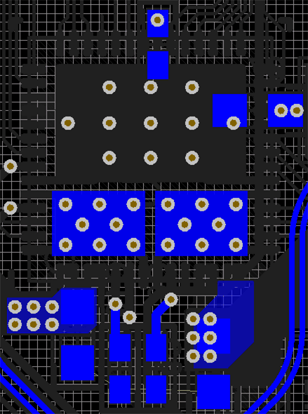
The figures below show the pours used in this example.
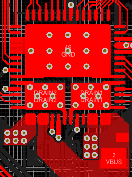
GUID-AE902461-03AE-4CF2-8E48-4DABE8C33D2A-low.gifFigure 11-8 Top Polygon Pours
GUID-65A605E8-FFB2-4136-B336-76DA70E6EBE3-low.gifFigure 11-9 Bottom Polygon Pours

For PP_CABLE, it is recommended to connect the capacitor to the pin with two vias. They should be placed side by side and as close to the pin as possible to allow for routing the CC lines.

Connect the bottom side VIN_3V3 and LDO_3V3 capacitors with traces through a via. The vias should have a straight connection to the respective pins. LDO_1V8 is connected through a via on the outside of the pin and connected with a trace on the bottom side capacitor.