ZHCSJP1B May 2019 – October 2022 TPS65987DDJ
PRODUCTION DATA
- 1 特性
- 2 应用
- 3 说明
- 4 Revision History
- 5 Pin Configuration and Functions
-
6 Specifications
- 6.1 Absolute Maximum Ratings
- 6.2 ESD Ratings
- 6.3 Recommended Operating Conditions
- 6.4 Thermal Information
- 6.5 Power Supply Requirements and Characteristics
- 6.6 Power Consumption Characteristics
- 6.7 Power Switch Characteristics
- 6.8 Cable Detection Characteristics
- 6.9 USB-PD Baseband Signal Requirements and Characteristics
- 6.10 BC1.2 Characteristics
- 6.11 Thermal Shutdown Characteristics
- 6.12 Oscillator Characteristics
- 6.13 I/O Characteristics
- 6.14 I2C Requirements and Characteristics
- 6.15 SPI Controller Timing Requirements
- 6.16 HPD Timing Requirements
- 6.17 Typical Characteristics
- 7 Parameter Measurement Information
-
8 Detailed Description
- 8.1 Overview
- 8.2 Functional Block Diagram
- 8.3
Feature Description
- 8.3.1 USB-PD Physical Layer
- 8.3.2 Power Management
- 8.3.3 Port Power Switches
- 8.3.4 Cable Plug and Orientation Detection
- 8.3.5 Dead Battery Operation
- 8.3.6 Battery Charger Detection and Advertisement
- 8.3.7 ADC
- 8.3.8 DisplayPort HPD
- 8.3.9 Digital Interfaces
- 8.3.10 Digital Core
- 8.3.11 I2C Interfaces
- 8.3.12 SPI Controller Interface
- 8.3.13 Thermal Shutdown
- 8.3.14 Oscillators
- 8.4 Device Functional Modes
-
9 Application and Implementation
- 9.1 Application Information
- 9.2
Typical Applications
- 9.2.1 Type-C VBUS Design Considerations
- 9.2.2 Notebook Design Supporting PD Charging
- 10Power Supply Recommendations
- 11Layout
- 12Device and Documentation Support
- 13Mechanical, Packaging, and Orderable Information
11.6 Thermal Dissipation for FET Drain Pads
The TPS65987DDJ contains two internal FETs. To assist with thermal dissipation of these FETs, the drains of the FETs are connected to two metal pads underneath the IC. When completing a board layout for the TPS65987DDJ, it is important to provide copper pours on the top and bottom layer of the PCB for the thermal pads of each FET.
When looking at the footprint for the TPS65987DDJ, pins 57 and 58 are two smaller pads underneath the device. These are the drain pads for the two internal FETs. The dimensions are 1.75 mil x 2.6 mil and 1.75 mil x 2.55 mil for pins 57 and 58 respectively. Each of these FET pads should contain a minimum of six thermal vias through the PCB. This layout example contains 8 thermal vias through the PCB. On the bottom side of the PCB, the 1.75 mil x 2.6 mil and 1.75 mil x 2.55 mil thermal pads are mirrored to assist with thermal dissipation.
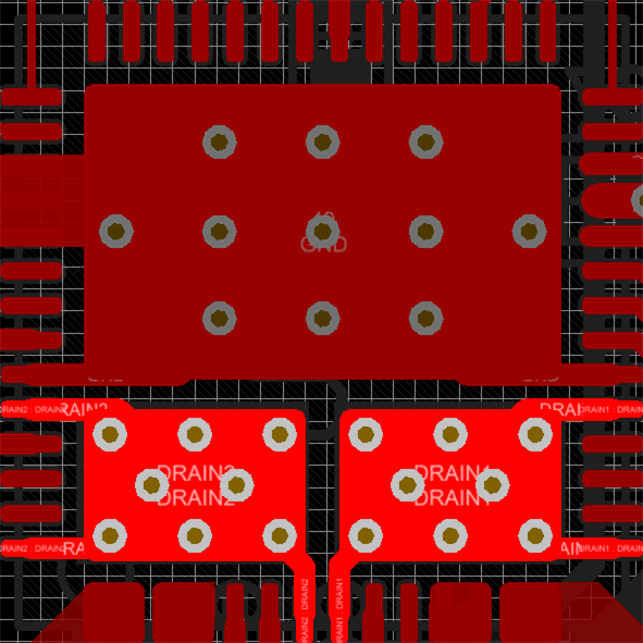
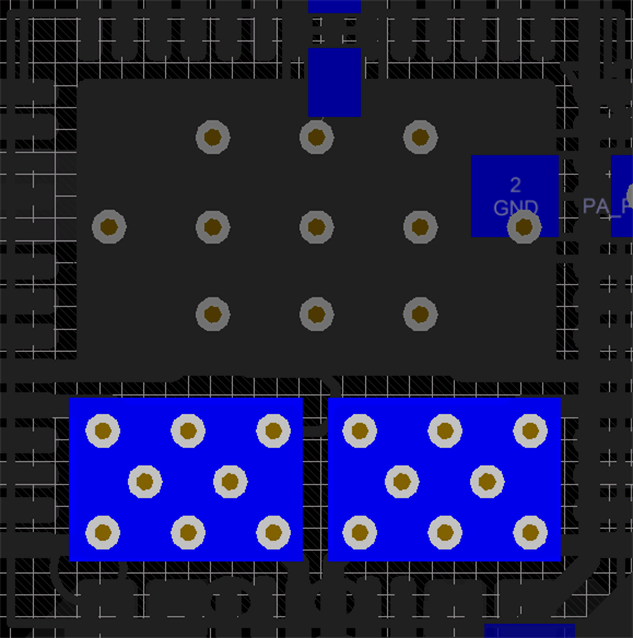
The figures below show the copper fills for the FET Drain pads.
 Figure 11-11 Top Layer FET Pads
 Figure 11-12 Bottom Layer FET Pads
As seen in the figures above, it is recommended to connect the Drain pins to their respective Drain pads underneath the IC. This will help with thermal dissipation by moving some of the heat away from the device. To further assist with thermal dissipation, it is possible to add copper fins on the top layer for both of the FET Drain Pads. When calculating the relative thermal dissipation, the first 3 mm of copper away from the device contribute largely to the thermal performance. Once the copper expands beyond 3 mm from the IC, there are diminishing returns in thermal performance.
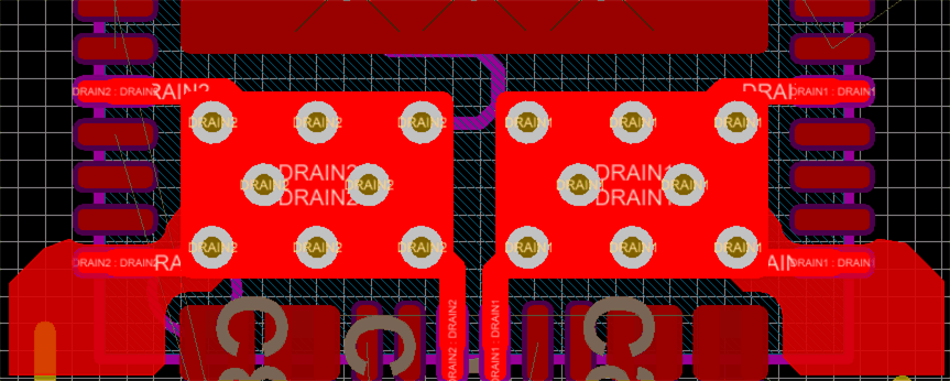
Figure 11-13 highlights an example with copper fins to improve thermal dissipation.
 Figure 11-13 Copper Fins on Drain Pad
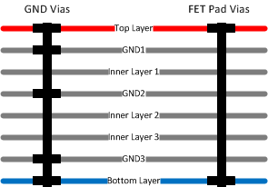
The thermal vias under each of the FET Drain Pads should be filled. Filling the vias will greatly improve the thermal dissipation on the FETs as there is significantly more copper that is connecting the top layer pad to the bottom layer copper. Alternatively, the vias can be epoxy filled but they will have higher thermal resistance. Each 8-/16-mil to 10-/20-mil via could have a thermal resistance ranging from 175°C/W to 200°C/W with board manufacturing variation. When doing thermal calculations it is recommended to use the worst case 200°C/W which will give a set of six vias a thermal resistance of approximately 33°C/W from the top to bottom pad. The vias in the FET pads should only be connected to copper pads on the top and bottom layers of the PCB. These should not be connected to GND. Refer to the image below to see which layers should be connected for the GND vias and FET Pad vias.
Figure 11-7 shows a common stack-up for systems that require Super Speed and high power routing.
 Figure 11-14 PCB Stack-Up