ZHCSJP1B
May 2019 – October 2022
TPS65987DDJ
PRODUCTION DATA
1
特性
2
应用
3
说明
4
Revision History
5
Pin Configuration and Functions
6
Specifications
6.1
Absolute Maximum Ratings
6.2
ESD Ratings
6.3
Recommended Operating Conditions
6.4
Thermal Information
6.5
Power Supply Requirements and Characteristics
6.6
Power Consumption Characteristics
6.7
Power Switch Characteristics
6.8
Cable Detection Characteristics
6.9
USB-PD Baseband Signal Requirements and Characteristics
6.10
BC1.2 Characteristics
6.11
Thermal Shutdown Characteristics
6.12
Oscillator Characteristics
6.13
I/O Characteristics
6.14
I2C Requirements and Characteristics
6.15
SPI Controller Timing Requirements
6.16
HPD Timing Requirements
6.17
Typical Characteristics
7
Parameter Measurement Information
8
Detailed Description
8.1
Overview
8.2
Functional Block Diagram
8.3
Feature Description
8.3.1
USB-PD Physical Layer
8.3.1.1
USB-PD Encoding and Signaling
8.3.1.2
USB-PD Bi-Phase Marked Coding
8.3.1.3
USB-PD Transmit (TX) and Receive (Rx) Masks
8.3.1.4
USB-PD BMC Transmitter
8.3.1.5
USB-PD BMC Receiver
8.3.2
Power Management
8.3.2.1
Power-On And Supervisory Functions
8.3.2.2
VBUS LDO
8.3.2.3
Supply Switch Over
8.3.3
Port Power Switches
8.3.3.1
PP_HV Power Switch
8.3.3.1.1
PP_HV Overcurrent Clamp
8.3.3.1.2
PP_HV Overcurrent Protection
8.3.3.1.3
PP_HV OVP and UVP
8.3.3.1.4
PP_HV Reverse Current Protection
8.3.3.2
Schottky for Current Surge Protection
8.3.3.3
PP_EXT Power Path Control
8.3.3.4
PP_CABLE Power Switch
8.3.3.4.1
PP_CABLE Overcurrent Protection
8.3.3.4.2
PP_CABLE Input Good Monitor
8.3.3.5
VBUS Transition to VSAFE5V
8.3.3.6
VBUS Transition to VSAFE0V
8.3.4
Cable Plug and Orientation Detection
8.3.4.1
Configured as a DFP
8.3.4.2
Configured as a UFP
8.3.4.3
Configured as a DRP
8.3.4.4
Fast Role Swap Signaling
8.3.5
Dead Battery Operation
8.3.5.1
Dead Battery Advertisement
8.3.5.2
BUSPOWER (ADCIN1)
8.3.6
Battery Charger Detection and Advertisement
8.3.6.1
BC1.2 Data Contact Detect
8.3.6.2
BC1.2 Primary and Secondary Detection
8.3.6.3
Charging Downstream Port Advertisement
8.3.6.4
Dedicated Charging Port Advertisement
8.3.6.5
2.7-V Divider3 Mode Advertisement
8.3.6.6
1.2-V Mode Advertisement
8.3.6.7
DCP Auto Mode Advertisement
8.3.7
ADC
8.3.8
DisplayPort HPD
8.3.9
Digital Interfaces
8.3.9.1
General GPIO
8.3.9.2
I2C
8.3.9.3
SPI
8.3.10
Digital Core
8.3.11
I2C Interfaces
8.3.11.1
I2C Interface Description
8.3.11.2
I2C Clock Stretching
8.3.11.3
I2C Address Setting
8.3.11.4
Unique Address Interface
8.3.11.5
I2C Pin Address Setting (ADCIN2)
8.3.12
SPI Controller Interface
8.3.13
Thermal Shutdown
8.3.14
Oscillators
8.4
Device Functional Modes
8.4.1
Boot
8.4.2
Power States
9
Application and Implementation
9.1
Application Information
9.2
Typical Applications
9.2.1
Type-C VBUS Design Considerations
9.2.1.1
Design Requirements
9.2.1.2
Detailed Design Procedure
9.2.1.2.1
Type-C Connector VBUS Capacitors
9.2.1.2.2
VBUS Schottky and TVS Diodes
9.2.1.2.3
VBUS Snubber Circuit
9.2.1.3
Application Curves
9.2.2
Notebook Design Supporting PD Charging
9.2.2.1
USB and DisplayPort Notebook Supporting PD Charging
9.2.2.1.1
Design Requirements
9.2.2.1.2
Detailed Design Procedure
9.2.2.1.2.1
USB Power Delivery Source Capabilities
9.2.2.1.2.2
USB Power Delivery Sink Capabilities
9.2.2.1.2.3
f
9.2.2.1.2.4
TUSB1046 Super Speed Mux GPIO Control
9.2.2.2
Thunderbolt Notebook Supporting PD Charging
9.2.2.2.1
Design Requirements
9.2.2.2.2
Detailed Design Procedure
9.2.2.2.2.1
USB Power Delivery Source Capabilities
9.2.2.2.2.2
USB Power Delivery Sink Capabilities
9.2.2.2.2.3
Thunderbolt Supported Data Modes
9.2.2.2.2.4
RESETN
9.2.2.2.2.5
I2C Design Requirements
9.2.2.2.2.6
TS3DS10224 SBU Mux for AUX and LSTX/RX
9.2.2.2.2.7
Thunderbolt Flash Options
9.2.2.3
USB and DisplayPort Dock with Bus-Powered and Self-Powered Support
9.2.2.3.1
Design Requirements
9.2.2.3.2
Detailed Design Procedure
9.2.2.3.2.1
USB Power Delivery Source Capabilities
9.2.2.3.2.2
USB Power Delivery Sink Capabilities
9.2.2.3.2.3
USB and DisplayPort Supported Data Modes
9.2.2.3.2.4
TUSB1064 Super Speed Mux GPIO Control
10
Power Supply Recommendations
10.1
3.3-V Power
10.1.1
VIN_3V3 Input Switch
10.1.2
VBUS 3.3-V LDO
10.2
1.8-V Power
10.3
Recommended Supply Load Capacitance
11
Layout
11.1
Layout Guidelines
11.1.1
Top TPS65987DDJ Placement and Bottom Component Placement and Layout
11.2
Layout Example
11.3
Component Placement
11.4
Routing PP_HV1/2, VBUS, PP_CABLE, VIN_3V3, LDO_3V3, LDO_1V8
11.5
Routing CC and GPIO
11.6
Thermal Dissipation for FET Drain Pads
11.7
USB2 Recommended Routing For BC1.2 Detection/Advertisement
12
Device and Documentation Support
12.1
Device Support
12.1.1
第三方米6体育平台手机版_好二三四免责声明
12.1.2
Firmware Warranty Disclaimer
12.2
Documentation Support
12.2.1
Related Documentation
12.3
接收文档更新通知
12.4
支持资源
12.5
Trademarks
12.6
Electrostatic Discharge Caution
12.7
术语表
13
Mechanical, Packaging, and Orderable Information
封装选项
机械数据 (封装 | 引脚)
RSH|56
MPQF191C
散热焊盘机械数据 (封装 | 引脚)
RSH|56
QFND570A
订购信息
zhcsjp1b_oa
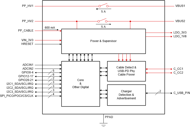
8.2
Functional Block Diagram
千亿体育app官网登录(中国)官方网站IOS/安卓通用版/手机APP
|
米乐app下载官网(中国)|ios|Android/通用版APP最新版
|
米乐|米乐·M6(中国大陆)官方网站
|
千亿体育登陆地址
|
华体会体育(中国)HTH·官方网站
|
千赢qy国际_全站最新版千赢qy国际V6.2.14安卓/IOS下载
|
18新利网v1.2.5|中国官方网站
|
bob电竞真人(中国官网)安卓/ios苹果/电脑版【1.97.95版下载】
|
千亿体育app官方下载(中国)官方网站IOS/安卓/手机APP下载安装
|