ZHCSLZ7B September 2020 – October 2022 TPS65987DDK
PRODUCTION DATA
- 1 特性
- 2 应用
- 3 说明
- 4 Revision History
- 5 Pin Configuration and Functions
-
6 Specifications
- 6.1 Absolute Maximum Ratings
- 6.2 ESD Ratings
- 6.3 Recommended Operating Conditions
- 6.4 Thermal Information
- 6.5 Power Supply Requirements and Characteristics
- 6.6 Power Consumption Characteristics
- 6.7 Power Switch Characteristics
- 6.8 Cable Detection Characteristics
- 6.9 USB-PD Baseband Signal Requirements and Characteristics
- 6.10 Thermal Shutdown Characteristics
- 6.11 Oscillator Characteristics
- 6.12 I/O Characteristics
- 6.13 I2C Requirements and Characteristics
- 6.14 SPI Controller Timing Requirements
- 6.15 HPD Timing Requirements
- 6.16 Typical Characteristics
- 7 Parameter Measurement Information
-
8 Detailed Description
- 8.1 Overview
- 8.2 Functional Block Diagram
- 8.3
Feature Description
- 8.3.1 USB-PD Physical Layer
- 8.3.2 Power Management
- 8.3.3 Port Power Switches
- 8.3.4 Cable Plug and Orientation Detection
- 8.3.5 Dead Battery Operation
- 8.3.6 ADC
- 8.3.7 DisplayPort HPD
- 8.3.8 Digital Interfaces
- 8.3.9 Digital Core
- 8.3.10 I2C Interfaces
- 8.3.11 SPI Controller Interface
- 8.3.12 Thermal Shutdown
- 8.3.13 Oscillators
- 8.4 Device Functional Modes
- 9 Application and Implementation
- 10Power Supply Recommendations
- 11Layout
- 12Device and Documentation Support
- 13Mechanical, Packaging, and Orderable Information
8.3.8.1 General GPIO
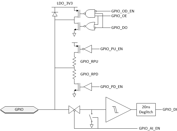
Figure 8-18 shows the GPIO I/O buffer for all GPIOn pins. GPIOn pins can be mapped to USB Type-C, USB PD, and application-specific events to control other ICs, interrupt a host processor, or receive input from another IC. This buffer is configurable to be a push-pull output, a weak push-pull, or open drain output. When configured as an input, the signal can be a de-glitched digital input . The push-pull output is a simple CMOS output with independent pull-down control allowing open-drain connections. The weak push-pull is also a CMOS output, but with GPIO_RPU resistance in series with the drain. The supply voltage to the output buffer is LDO_3V3 and LDO_1V8 to the input buffer. When interfacing with non 3.3-V I/O devices the output buffer may be configured as an open drain output and an external pull-up resistor attached to the GPIO pin. The pull-up and pull-down output drivers are independently controlled from the input and are enabled or disabled via application code in the digital core.
 Figure 8-18 General GPIO Buffer