ZHCSIY2B July 2018 – August 2021 TPS65988
PRODUCTION DATA
- 1 特性
- 2 应用
- 3 说明
- 4 Revision History
- 5 Pin Configuration and Functions
-
6 Specifications
- 6.1 Absolute Maximum Ratings
- 6.2 ESD Ratings
- 6.3 Recommended Operating Conditions
- 6.4 Thermal Information
- 6.5 Power Supply Requirements and Characteristics
- 6.6 Power Consumption Characteristics
- 6.7 Power Switch Characteristics
- 6.8 Cable Detection Characteristics
- 6.9 USB-PD Baseband Signal Requirements and Characteristics
- 6.10 BC1.2 Characteristics
- 6.11 Thermal Shutdown Characteristics
- 6.12 Oscillator Characteristics
- 6.13 I/O Characteristics
- 6.14 PWM Driver Characteristics
- 6.15 I2C Requirements and Characteristics
- 6.16 SPI Controller Timing Requirements
- 6.17 HPD Timing Requirements
- 6.18 Typical Characteristics
- 7 Parameter Measurement Information
-
8 Detailed Description
- 8.1 Overview
- 8.2 Functional Block Diagram
- 8.3
Feature Description
- 8.3.1 USB-PD Physical Layer
- 8.3.2 Power Management
- 8.3.3 Port Power Switches
- 8.3.4 Cable Plug and Orientation Detection
- 8.3.5 Dead Battery Operation
- 8.3.6 Battery Charger Detection and Advertisement
- 8.3.7 ADC
- 8.3.8 DisplayPort HPD
- 8.3.9 Digital Interfaces
- 8.3.10 PWM Driver
- 8.3.11 Digital Core
- 8.3.12 I2C Interfaces
- 8.3.13 SPI Controller Interface
- 8.3.14 Thermal Shutdown
- 8.3.15 Oscillators
- 8.4 Device Functional Modes
-
9 Application and Implementation
- 9.1 Application Information
- 9.2
Typical Applications
- 9.2.1 Type-C VBUS Design Considerations
- 9.2.2 Dual Port Thunderbolt Notebook with AR Supporting USB PD Charging
- 9.2.3 Dual Port USB & Displayport Notebook Supporting PD Charging
- 9.2.4 USB Type-C & PD Monitor/Dock
- 10Power Supply Recommendations
-
11Layout
- 11.1 Layout Guidelines
- 11.2 Layout Example
- 11.3 Stack-Up and Design Rules
- 11.4 Main Component Placement
- 11.5 1.4 Super Speed Type-C Connectors
- 11.6 Capacitor Placement
- 11.7 CC1/2 Capacitors & ADCIN1/2 Resistors
- 11.8 CC & SBU Protection Placement
- 11.9 CC Routing
- 11.10 DRAIN1 and DRAIN2 Pad Pours
- 11.11 USB2 Routing for ESD Protection and BC1.2
- 11.12 VBUS Routing
- 11.13 Completed Layout
- 11.14 Power Dissipation
- 12Device and Documentation Support
- 13Mechanical, Packaging, and Orderable Information
9.2.1.2.1.2 Discrete Power Path
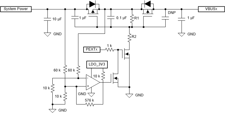
The recommended discrete power path includes reverse current protection to disable the power path when both sink paths are enabled at different PD contracts. In Figure 9-1 a comparator is used to force disable the external power path when the common source voltage is higher than the system voltage. The comparator circuit has hysteresis added to prevent any oscillations when the system voltage is very close to the common source voltage. The NMOS driven by the comparator will pull the PEXTx to GND when the common source voltage is higher than the system power and the 1k in series will limit the current drawn from the PEXTx GPIO. The comparator is powered from LDO_3V3 on the TPS65988 which mean that even in dead battery operation the comparator circuit will remain active regardless of the state of PEXTx. For lower power consumption from VBUS the voltage dividers for the comparator inputs can use higher resistance values.
 Figure 9-1 Recommended Sink Power Path
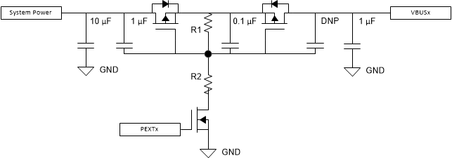
The simplest discrete power path does not have reverse current protection and relies on either on the configuration to only enable the power path with the highest power PD contract or on the EC to enable and disable the power path. This simple power path has some limitations as it will always be fully on or fully off and both paths cannot be enabled at the same time. Figure 9-2 shows the design.
 Figure 9-2 Simple Sink Power Path
For both discrete implementations the R1 and R2 divider should be selected to reach the PMOS threshold (Vgs) at 5 V and 20 V to insure the common source PMOS are completely on. When the sink path is enabled the R1 and R2 resistance will draw current from VBUS. For systems that need to meet low power requirements it is recommended to use higher resistance values for R1 and R2 but this will slow how fast the external sink path turns off and on. A R1 = 100k and R2 = 10k is a good medium that will draw around 3.6mW from VBUS at 20 V and will create enough VGS for most PMOS.