ZHCSLZ8A September 2020 – August 2021 TPS65988DK
PRODUCTION DATA
- 1 特性
- 2 应用
- 3 说明
- 4 Revision History
- 5 Pin Configuration and Functions
-
6 Specifications
- 6.1 Absolute Maximum Ratings
- 6.2 ESD Ratings
- 6.3 Recommended Operating Conditions
- 6.4 Thermal Information
- 6.5 Power Supply Requirements and Characteristics
- 6.6 Power Consumption Characteristics
- 6.7 Power Switch Characteristics
- 6.8 Cable Detection Characteristics
- 6.9 USB-PD Baseband Signal Requirements and Characteristics
- 6.10 Thermal Shutdown Characteristics
- 6.11 Oscillator Characteristics
- 6.12 I/O Characteristics
- 6.13 I2C Requirements and Characteristics
- 6.14 SPI Controller Timing Requirements
- 6.15 HPD Timing Requirements
- 6.16 Typical Characteristics
- 7 Parameter Measurement Information
-
8 Detailed Description
- 8.1 Overview
- 8.2 Functional Block Diagram
- 8.3
Feature Description
- 8.3.1 USB-PD Physical Layer
- 8.3.2 Power Management
- 8.3.3 Port Power Switches
- 8.3.4 Cable Plug and Orientation Detection
- 8.3.5 Dead Battery Operation
- 8.3.6 ADC
- 8.3.7 DisplayPort HPD
- 8.3.8 Digital Interfaces
- 8.3.9 Digital Core
- 8.3.10 I2C Interfaces
- 8.3.11 SPI Controller Interface
- 8.3.12 Thermal Shutdown
- 8.3.13 Oscillators
- 8.4 Device Functional Modes
- 9 Application and Implementation
- 10Power Supply Recommendations
-
11Layout
- 11.1 Layout Guidelines
- 11.2 Layout Example
- 11.3 Stack-up and Design Rules
- 11.4 Main Component Placement
- 11.5 Super Speed Type-C Connectors
- 11.6 Capacitor Placement
- 11.7 CC1/2 Capacitors & ADCIN1/2 Resistors
- 11.8 CC and SBU Protection Placement
- 11.9 CC Routing
- 11.10 DRAIN1 and DRAIN2 Pad Pours
- 11.11 VBUS Routing
- 11.12 Completed Layout
- 11.13 Power Dissipation
- 12Device and Documentation Support
- 13Mechanical, Packaging, and Orderable Information
8.3.5.1 Dead Battery Advertisement
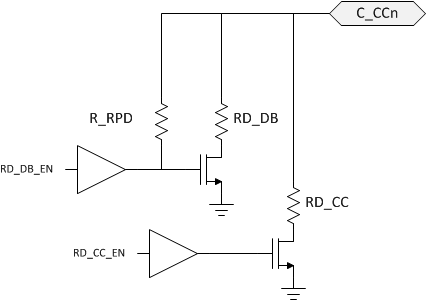
The TPS65988DK supports booting from no-battery or dead-battery conditions by receiving power from VBUS. Type-C USB ports require a sink to present Rd on the CC pin before a USB Type-C source provides a voltage on VBUS. The TPS65988DK hardware is configured to present this Rd during a dead-battery or no-battery condition. Additional circuitry provides a mechanism to turn off this Rd once the device no longer requires power from VBUS. Figure 8-16 shows the configuration of the C_CCn pins, and elaborates on the basic cable plug and orientation detection block shown in Figure 8-14. A resistance R_RPD is connected to the gate of the pull-down FET on each C_CCn pin. During normal operation when configured as a sink, RD is RD_CC; however, while dead-battery or no-battery conditions exist, the resistance is un-trimmed and is RD_DB. When RD_DB is presented during dead-battery or no-battery, application code switches to RD_CC.
 Figure 8-16 Dead Battery Pull-Down Resistor
In this case, the gate driver for the pull-down FET is Hi-Z at its output. When an external connection pulls up on C_CCn (the case when connected to a DFP advertising with a pull-up resistance Rp or pull-up current), the connection through R_RPD pulls up on the FET gate turning on the pull-down through RD_DB. In this condition, the C_CCn pin acts as a clamp VTH_DB in series with the resistance RD_DB.