ZHCSDI0A October 2014 – March 2015 TPS706
PRODUCTION DATA.
- 1 特性
- 2 应用
- 3 说明
- 4 修订历史记录
- 5 Pin Configuration and Functions
- 6 Specifications
- 7 Detailed Description
- 8 Application and Implementation
- 9 Power Supply Recommendations
- 10Layout
- 11器件和文档支持
- 12机械封装和可订购信息
封装选项
机械数据 (封装 | 引脚)
散热焊盘机械数据 (封装 | 引脚)
- DRV|6
订购信息
8 Application and Implementation
NOTE
Information in the following applications sections is not part of the TI component specification, and TI does not warrant its accuracy or completeness. TI’s customers are responsible for determining suitability of components for their purposes. Customers should validate and test their design implementation to confirm system functionality.
8.1 Application Information
The TPS706 consumes low quiescent current and delivers excellent line and load transient performance. This performance, combined with low noise and good PSRR with little (VIN – VOUT) headroom, makes these devices ideal for RF portable applications, current limit, and thermal protection. The TPS706 devices are specified from –40°C to 125°C.
8.1.1 Input and Output Capacitor Considerations
The TPS706 devices are stable with output capacitors with an effective capacitance of 2.0 μF or greater for output voltages below 1.5 V. For output voltages equal or greater than 1.5 V, the minimum effective capacitance for stability is 1.5 µF. The maximum capacitance for stability is 47 µF. The equivalent series resistance (ESR) of the output capacitor must be between 0 Ω and 0.2 Ω for stability.
The effective capacitance is the minimum capacitance value of a capacitor after taking into account variations resulting from tolerances, temperature, and dc bias effects. X5R- and X7R-type ceramic capacitors are recommended because these capacitors have minimal variation in value and ESR over temperature.
Although an input capacitor is not required for stability, good analog design practice is to connect a 0.1-µF to
2.2-µF capacitor from IN to GND. This capacitor counteracts reactive input sources and improves transient response, input ripple rejection, and PSRR.
8.1.2 Dropout Voltage
The TPS706 uses a PMOS pass transistor to achieve low dropout. When (VIN – VOUT) is less than the dropout voltage (VDO), the PMOS pass device is in the linear region of operation and the input-to-output resistance is the RDS(ON) of the PMOS pass element. VDO approximately scales with the output current because the PMOS device functions like a resistor in dropout.
The ground pin current of many linear voltage regulators increases substantially when the device is operated in dropout. This increase in ground pin current while operating in dropout can be several orders of magnitude larger than when the device is not in dropout. The TPS706 employs a special control loop that limits the increase in ground pin current while operating in dropout. This functionality allows for the most efficient operation while in dropout conditions that can greatly increase battery run times.
8.1.3 Transient Response
As with any regulator, increasing the output capacitor size reduces over- and undershoot magnitude, but increases transient response duration.
8.2 Typical Application
 Figure 30. 3.3-V, Low-IQ Rail
8.2.1 Design Requirements
Table 2 summarizes the design requirements for Figure 30.
Table 2. Design Requirements for a 3.3-V, Low-IQ Rail Application
| PARAMETER | DESIGN SPECIFICATION |
|---|---|
| VIN | 4.3 V |
| VOUT | 3.3 V |
| I(IN) (no load) | < 5 µA |
| IOUT (max) | 150 mA |
8.2.2 Detailed Design Procedure
Select a 2.2-µF, 10-V X7R output capacitor to satisfy the minimum output capacitance requirement with a 3.3-V dc bias.
Select a 1.0-µF, 6.3-V X7R input capacitor to provide input noise filtering and eliminate high-frequency voltage transients.
8.2.3 Application Curves

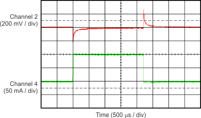
| Channel 2 = VOUT, channel 4 = IOUT, VIN = 4.3 V |

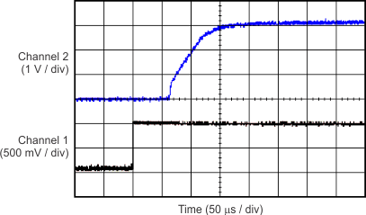
| Channel 1 = EN, channel 2 = VOUT, VIN = 4.3 V, COUT = 2.2 µF, TPS70633 |