ZHCSC15C December   2013  – June 2018 TPS709-Q1

PRODUCTION DATA.  

  1. 特性
  2. 应用
  3. 说明
    1.     Device Images
      1.      典型应用电路
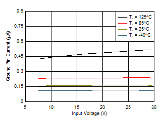
      2.      接地电流与 VIN 和温度间的关系
  4. 修订历史记录
  5. Pin Configuration and Functions
    1.     Pin Functions
  6. Specifications
    1. 6.1 Absolute Maximum Ratings
    2. 6.2 ESD Ratings
    3. 6.3 Recommended Operating Conditions
    4. 6.4 Thermal Information
    5. 6.5 Electrical Characteristics
    6. 6.6 Timing Requirements
    7. 6.7 Typical Characteristics
  7. Detailed Description
    1. 7.1 Overview
    2. 7.2 Functional Block Diagram
    3. 7.3 Feature Description
      1. 7.3.1 Undervoltage Lockout (UVLO)
      2. 7.3.2 Shutdown
      3. 7.3.3 Reverse Current Protection
      4. 7.3.4 Internal Current Limit
      5. 7.3.5 Thermal Protection
    4. 7.4 Device Functional Modes
      1. 7.4.1 Normal Operation
      2. 7.4.2 Dropout Operation
      3. 7.4.3 Disabled
  8. Application and Implementation
    1. 8.1 Application Information
      1. 8.1.1 Input and Output Capacitor Considerations
      2. 8.1.2 Dropout Voltage
      3. 8.1.3 Transient Response
    2. 8.2 Typical Application
      1. 8.2.1 Design Requirements
      2. 8.2.2 Detailed Design Procedure
      3. 8.2.3 Application Curves
  9. Power Supply Recommendations
  10. 10Layout
    1. 10.1 Layout Guidelines
      1. 10.1.1 Board Layout Recommendations to Improve PSRR and Noise Performance
      2. 10.1.2 Power Dissipation
    2. 10.2 Layout Examples
  11. 11器件和文档支持
    1. 11.1 器件支持
      1. 11.1.1 开发支持
        1. 11.1.1.1 评估模块
        2. 11.1.1.2 Spice 模型
      2. 11.1.2 器件命名规则
    2. 11.2 文档支持
      1. 11.2.1 相关文档
    3. 11.3 接收文档更新通知
    4. 11.4 社区资源
    5. 11.5 商标
    6. 11.6 静电放电警告
    7. 11.7 术语表
  12. 12机械、封装和可订购信息

封装选项

请参考 PDF 数据表获取器件具体的封装图。

机械数据 (封装 | 引脚)
  • DBV|5
  • DRV|6
散热焊盘机械数据 (封装 | 引脚)
订购信息

Typical Characteristics

Over operating temperature range (TJ = –40°C to 125°C), IOUT = 10 mA, VEN = 2 V, COUT = 2.2 μF, and VIN = VOUT(nom) + 1 V or 2.7 V (whichever is greater), unless otherwise noted. Typical values are at TJ = 25°C.
TPS709-Q1 D001_SLVSCE6.gif
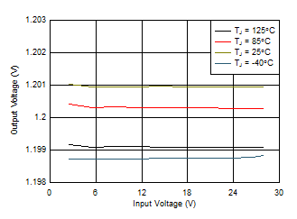
Figure 1. 1.2-V Line Regulation vs VIN and Temperature
TPS709-Q1 D003_SLVSCE6.gif
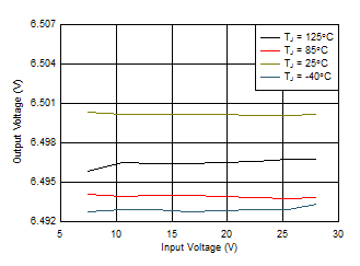
Figure 3. 6.5-V Line Regulation vs VIN and Temperature
TPS709-Q1 D005_SLVSCE6.gif
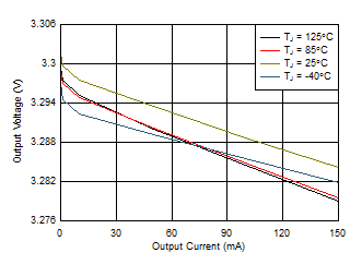
Figure 5. 3.3-V Load Regulation vs IOUT and Temperature
TPS709-Q1 D007_SLVSCE6.gif
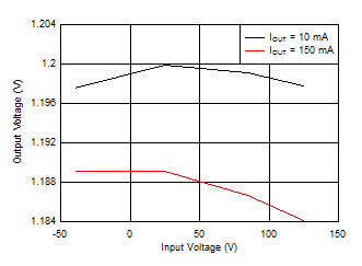
Figure 7. 1.2-V Output Voltage vs Temperature
TPS709-Q1 D009_SLVSCE6.gif
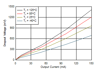
Figure 9. 3.3-V Dropout Voltage vs IOUT and Temperature
TPS709-Q1 D011_SLVSCE6.gif
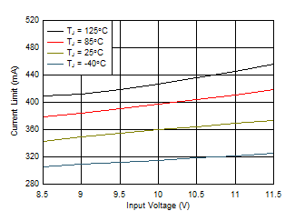
Figure 11. 1.2-V Current Limit vs VIN and Temperature
TPS709-Q1 D013_SLVSCE6.gif
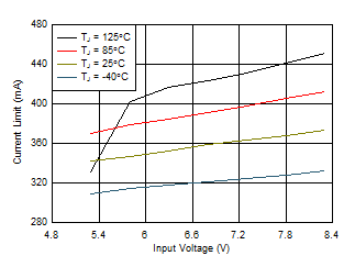
Figure 13. 6.5-V Current Limit vs VIN and Temperature
TPS709-Q1 D015_SLVSCE6.gif
Figure 15. 3.3-V Ground Pin Current vs VIN and
Temperature
TPS709-Q1 D017_SLVSCE6.gif
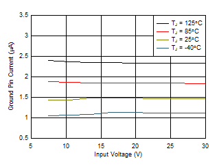
Figure 17. 3.3-V Ground Current vs VIN and
Temperature with EN Floating
TPS709-Q1 D019_SLVSCE6.gif
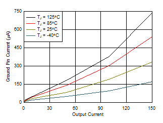
Figure 19. 3.3-V Ground Pin Current vs IOUT and
Temperature
TPS709-Q1 D021_SLVSCE6.gif
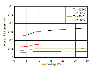
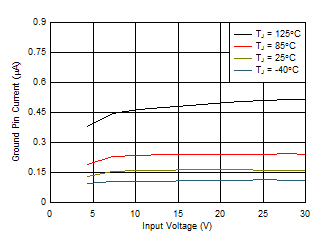
Figure 21. 1.2-V Shutdown Current vs VIN and Temperature
TPS709-Q1 D023_SLVSCE6.gif
Figure 23. 6.5-V Shutdown Current vs VIN and Temperature
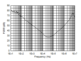
TPS709-Q1 D002_SBVS245.gif
Figure 25. Power-Supply Rejection Ratio vs Frequency
TPS709-Q1 G020_BVS245.gif
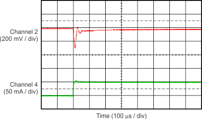
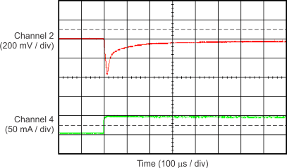
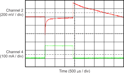
Channel 2 = VOUT, channel 4 = IOUT, VIN = 2.7 V
Figure 27. TPS70912-Q1 Load Transient (0 mA to 50 mA)
TPS709-Q1 G022_BVS245.gif
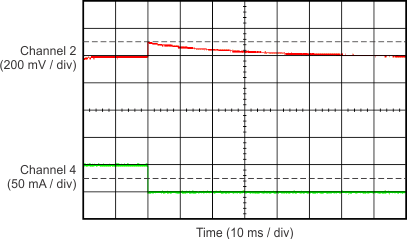
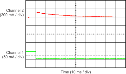
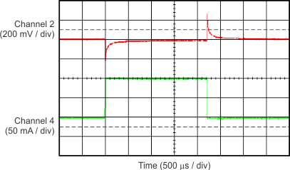
Channel 2 = VOUT, channel 4 = IOUT, VIN = 2.7 V
Figure 29. TPS70912-Q1 Load Transient (50 mA to 0 mA)
TPS709-Q1 G024_BVS245.gif
Channel 2 = VOUT, channel 4 = IOUT, VIN = 4.3 V
Figure 31. TPS70933-Q1 Load Transient (0 mA to 50 mA)
TPS709-Q1 G026_BVS245.gif
Channel 2 = VOUT, channel 4 = IOUT, VIN = 4.3 V
Figure 33. TPS70933-Q1 Load Transient (50 mA to 0 mA)
TPS709-Q1 G028_BVS245.gif
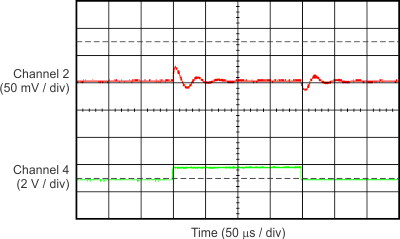
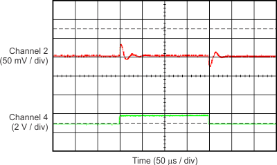
Channel 2 = VOUT, channel 4 = VIN, IOUT = 10 mA
Figure 35. TPS70912-Q1 Line Transient (2.7 V to 3.7 V)
TPS709-Q1 G030_BVS245.gif
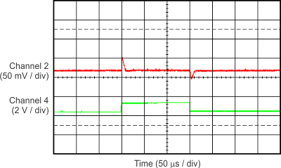
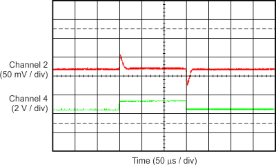
Channel 2 = VOUT, channel 4 = VIN, IOUT = 10 mA
Figure 37. TPS70933-Q1 Line Transient (4.3 V to 5.3 V)
TPS709-Q1 G032_BVS245.gif
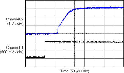
Channel 1 = EN, channel 2 = VOUT, VIN = 4.3 V, COUT = 2.2 µF, TPS70633
Figure 39. Power-Up with Enable
TPS709-Q1 G034_BVS245.gif
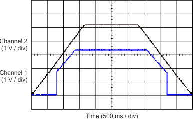
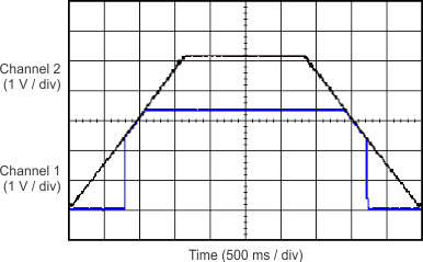
Channel 1 = VIN, channel 2 = VOUT, IOUT = 150 mA, TPS70633
Figure 41. Power-Up and Power-Down Response
TPS709-Q1 D002_SLVSCE6.gif
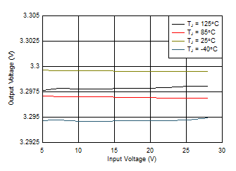
Figure 2. 3.3-V Line Regulation vs VIN and Temperature
TPS709-Q1 D004_SLVSCE6.gif
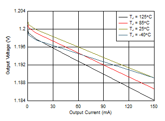
Figure 4. 1.2-V Load Regulation vs IOUT and Temperature
TPS709-Q1 D006_SLVSCE6.gif
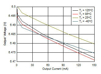
Figure 6. 6.5-V Load Regulation vs IOUT and Temperature
TPS709-Q1 D008_SLVSCE6.gif
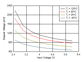
Figure 8. 6.5-V Dropout Voltage vs VIN and Temperature
TPS709-Q1 D010_SLVSCE6.gif
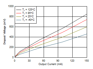
Figure 10. Dropout Voltage vs IOUT and Temperature
TPS709-Q1 D012_SLVSCE6.gif
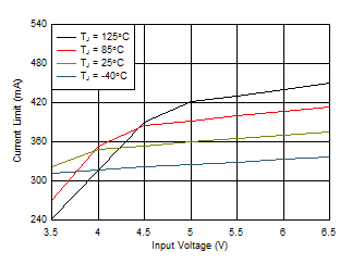
Figure 12. 3.3-V Current Limit vs VIN and Temperature
TPS709-Q1 D014_SLVSCE6.gif
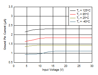
Figure 14. 1.2-V Ground Pin Current vs VIN and
Temperature
TPS709-Q1 D016_SLVSCE6.gif
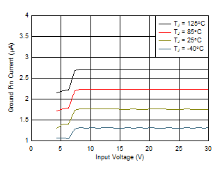
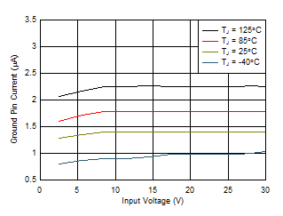
Figure 16. 6.5-V Ground Pin Current vs VIN and
Temperature
TPS709-Q1 D018_SLVSCE6.gif
Figure 18. 1.2-V Ground Pin Current vs IOUT and Temperature
TPS709-Q1 D020_SLVSCE6.gif
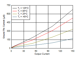
Figure 20. 6.5-V Ground Pin Current vs IOUT and Temperature
TPS709-Q1 D022_SLVSCE6.gif
Figure 22. 3.3-V Shutdown Current vs VIN and Temperature
TPS709-Q1 D024_SLVSCE6.gif
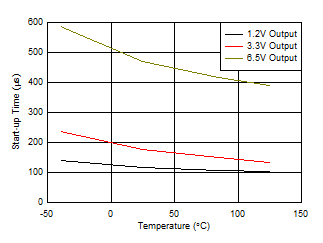
Figure 24. Start-Up Time vs Temperature
TPS709-Q1 D012_SBVS245.gif
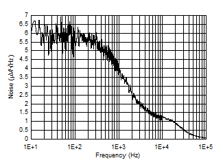
Figure 26. Noise
TPS709-Q1 G021_BVS245.gif
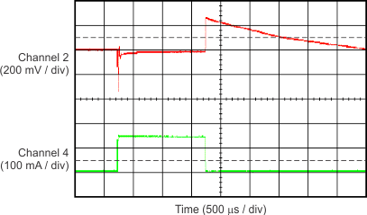
Channel 2 = VOUT, channel 4 = IOUT, VIN = 2.7 V
Figure 28. TPS70912-Q1 Load Transient (1 mA to 150 mA)
TPS709-Q1 G023_BVS245.gif
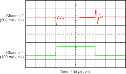
Channel 2 = VOUT, channel 4 = IOUT, VIN = 2.7 V
Figure 30. TPS70912-Q1 Load Transient (50 mA to 150 mA)
TPS709-Q1 G025_BVS245.gif
Channel 2 = VOUT, channel 4 = IOUT, VIN = 4.3 V
Figure 32. TPS70933-Q1 Load Transient (1 mA to 150 mA)
TPS709-Q1 G027_BVS245.gif
Channel 2 = VOUT, channel 4 = IOUT, VIN = 4.3 V
Figure 34. TPS70933-Q1 Load Transient (50 mA to 150 mA)
TPS709-Q1 G029_BVS245.gif
Channel 2 = VOUT, channel 4 = VIN, IOUT = 50 mA
Figure 36. TPS70912-Q1 Line Transient (2.7 V to 3.7 V)
TPS709-Q1 G031_BVS245.gif
Channel 2 = VOUT, channel 4 = VIN, IOUT = 50 mA
Figure 38. TPS70933-Q1 Line Transient (4.3 V to 5.3 V)
TPS709-Q1 G033_BVS245.gif
Channel 1 = VIN, channel 2 = VOUT, IOUT = 3 mA, TPS70633
Figure 40. Power-Up and Power-Down Response