ZHCS814H March   2012  – July 2021 TPS709

PRODUCTION DATA  

  1. 特性
  2. 应用
  3. 说明
  4. Revision History
  5. Pin Configuration and Functions
  6. Specifications
    1. 6.1 Absolute Maximum Ratings
    2. 6.2 ESD Ratings
    3. 6.3 Recommended Operating Conditions
    4. 6.4 Thermal Information
    5. 6.5 Electrical Characteristics
    6. 6.6 Typical Characteristics
  7. Detailed Description
    1. 7.1 Overview
    2. 7.2 Functional Block Diagram
    3. 7.3 Feature Description
      1. 7.3.1 Internal Current Limit
      2. 7.3.2 Dropout Voltage
      3. 7.3.3 Undervoltage Lockout (UVLO)
      4. 7.3.4 Reverse-Current Protection
    4. 7.4 Device Functional Modes
  8. Application and Implementation
    1. 8.1 Application Information
      1. 8.1.1 Input and Output Capacitor
      2. 8.1.2 Transient Response
    2. 8.2 Typical Application
      1. 8.2.1 Design Requirements
      2. 8.2.2 Detailed Design Procedure
      3. 8.2.3 Application Curves
  9. Power Supply Recommendations
    1. 9.1 Power Dissipation
  10. 10Layout
    1. 10.1 Layout Guidelines
      1. 10.1.1 Thermal Protection
    2. 10.2 Layout Example
  11. 11Device and Documentation Support
    1. 11.1 Device Support
      1. 11.1.1 Development Support
        1. 11.1.1.1 Evaluation Modules
        2. 11.1.1.2 Spice Models
      2. 11.1.2 Device Nomenclature
    2. 11.2 Documentation Support
      1. 11.2.1 Related Documentation
    3. 11.3 支持资源
    4. 11.4 Trademarks
    5. 11.5 Electrostatic Discharge Caution
    6. 11.6 术语表
  12. 12Mechanical, Packaging, and Orderable Information

封装选项

机械数据 (封装 | 引脚)
散热焊盘机械数据 (封装 | 引脚)
订购信息

Typical Characteristics

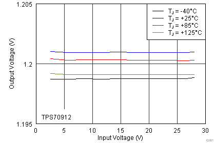
over operating temperature range (TJ = –40°C to 125°C), IOUT = 10 mA, VEN = 2 V, COUT = 2.2 μF, and VIN = VOUT(typ) + 1 V or 2.7 V (whichever is greater), unless otherwise noted; typical values are at TJ = 25°C
GUID-1E169A5A-E688-4897-95A7-087840284BA3-low.png
 
Figure 6-1 1.2-V Line Regulation vs VIN and Temperature
GUID-A17B4322-11DA-44A4-9165-EB4FE07798D9-low.png
 
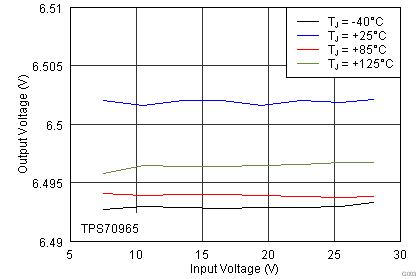
Figure 6-3 6.5-V Line Regulation vs VIN and Temperature
GUID-2C5FA17F-E227-4DD8-B0A8-4059005B0CE7-low.png
 
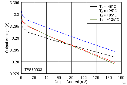
Figure 6-5 3.3-V Load Regulation vs IOUT and Temperature
GUID-89531BA9-B616-4E54-B7A0-A2459E081D6D-low.png
 
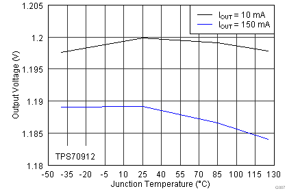
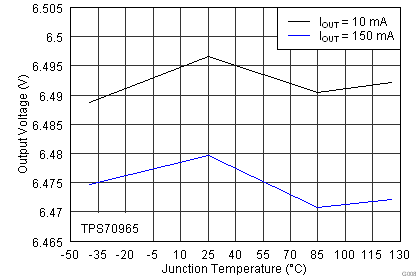
Figure 6-7 VOUT vs Temperature
GUID-F877F932-8333-4C0D-B250-23DFD452CAFC-low.png
 
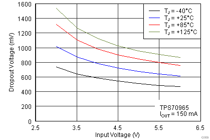
Figure 6-9 Dropout Voltage vs VIN and Temperature
GUID-51CD214F-A670-4A51-8EB9-C6DC1001775B-low.png
 
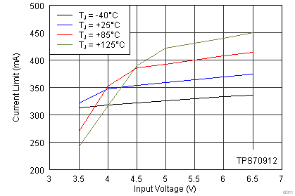
Figure 6-11 1.2-V Current Limit vs VIN and Temperature
GUID-6BFDC31D-4A9E-4942-AE12-0E6E120592DB-low.png
 
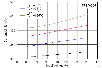
Figure 6-13 6.5-V Current Limit vs VIN and Temperature
GUID-9042A743-D015-42C4-88EE-B0F51A9BB681-low.png
 
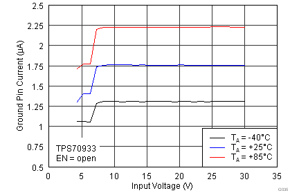
Figure 6-15 GND Current vs VIN and Temperature
GUID-13257F93-3D6E-40FA-A0B9-0DCB739C1312-low.png
 
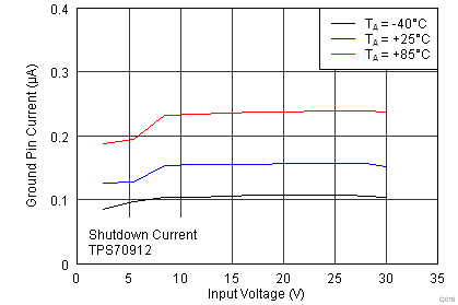
Figure 6-17 Shutdown Current vs VIN and Temperature
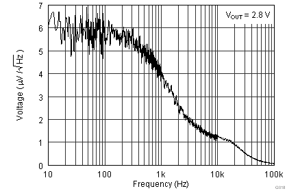
GUID-B338522A-CE67-4213-A5D8-090CC1D88D12-low.png
 
Figure 6-19 Noise
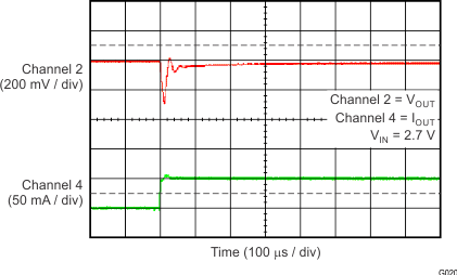
GUID-9D701BA7-65DB-4ED9-8F80-CBA62C85CF17-low.gif
 
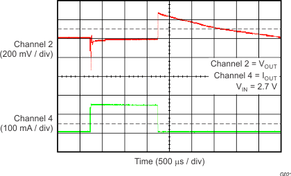
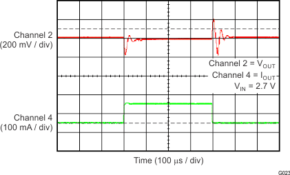
Figure 6-21 TPS70912 Load Transient
(0 mA to 50 mA)
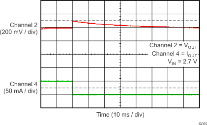
GUID-5CABDC4A-2C85-4CC7-A6D8-8F2426E4A1D8-low.gif
 
Figure 6-23 TPS70912 Load Transient
(50 mA to 0 mA)
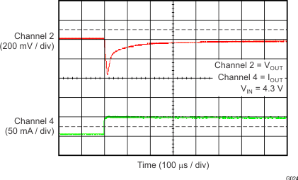
GUID-A506A31A-7E31-4390-9308-981A6AE3B445-low.gif
 
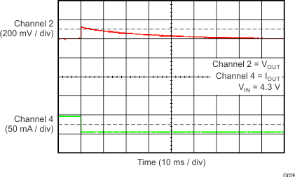
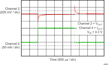
Figure 6-25 TPS70933 Load Transient
(0 mA to 50 mA)
GUID-7B12C200-CA7B-4BFA-AD6B-AA26D5D4B0E1-low.gif
 
Figure 6-27 TPS70933 Load Transient
(50 mA to 0 mA)
GUID-CAFA7D0C-0F61-493D-B406-938F2B3BE62C-low.gif
 
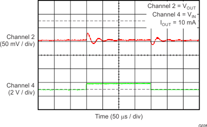
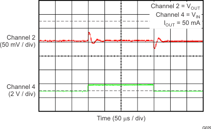
Figure 6-29 TPS70912 Line Transient
(2.7 V to 3.7 V)
GUID-8A463AC7-913F-4503-9499-45A8C284B8F0-low.gif
 
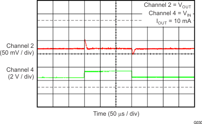
Figure 6-31 TPS70933 Line Transient
(4.3 V to 5.3 V)
GUID-59BD6006-1B85-451D-ABA2-7DA600575B43-low.gif
 
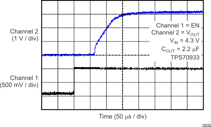
Figure 6-33 Power-Up With Enable
GUID-0046EA9C-A097-4FAA-9891-4E4318E9E8A3-low.gif
 
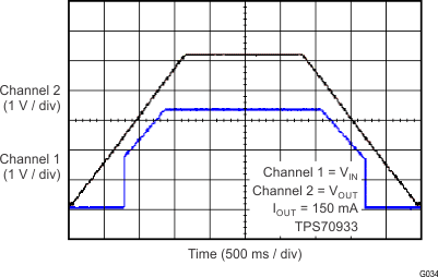
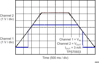
Figure 6-35 Power-Up and Power-Down Response
GUID-470B47ED-F848-412D-869C-9206A36FE3E7-low.png
 
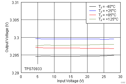
Figure 6-2 3.3-V Line Regulation vs VIN and Temperature
GUID-5F2BD572-5773-4CE2-BD7A-FBDD555904EC-low.png
 
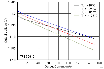
Figure 6-4 1.2-V Load Regulation vs IOUT and Temperature
GUID-3D750746-5134-43A3-923D-2F7D52B0CEEA-low.png
 
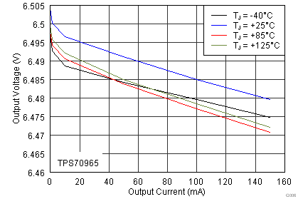
Figure 6-6 6.5-V Load Regulation vs IOUT and Temperature
GUID-9E0CAB9F-C40D-418A-B993-8C11A8AB311C-low.png
 
Figure 6-8 VOUT vs Temperature
GUID-47EE80FC-4DA9-40A2-A6C1-2FA1FCB47CED-low.png
 
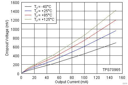
Figure 6-10 Dropout Voltage vs IOUT and Temperature
GUID-DCECBD33-972A-4345-A15B-FDE92CF4FFEB-low.png
 
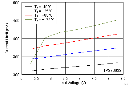
Figure 6-12 3.3-V Current Limit vs VIN and Temperature
GUID-18C6CF68-CA53-4BBD-BDC9-E1FD4F1DA4B8-low.png
 
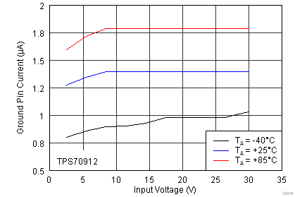
Figure 6-14 GND Current vs VIN and Temperature
GUID-5240283E-4674-45D2-B5FB-E920A33A420A-low.png
 
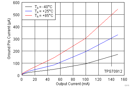
Figure 6-16 GND Current vs IOUT and Temperature
GUID-835D846B-3DC2-4E3A-9A13-488339830856-low.png
 
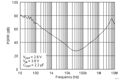
Figure 6-18 Power-Supply Rejection Ratio vs Frequency
GUID-C7050C7E-8B68-4124-A3D0-533553E09174-low.png
 
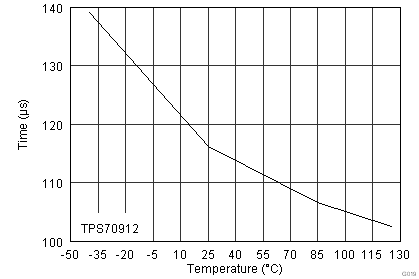
Figure 6-20 Start-Up Time vs Temperature
GUID-5440561B-2BD9-4DC7-A1CE-5C2D53F8C72C-low.gif
 
Figure 6-22 TPS70912 Load Transient
(1 mA to 150 mA)
GUID-6E758642-89F7-4A42-9E1F-F8E49A5B2F82-low.gif
 
Figure 6-24 TPS70912 Load Transient
(50 mA to 150 mA)
GUID-8E32BA1C-E54F-4AD9-A3C3-31D73D655F46-low.gif
 
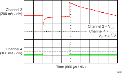
Figure 6-26 TPS70933 Load Transient
(1 mA to 150 mA)
GUID-19514912-BD0E-41CD-ACD7-ECE876C0144E-low.gif
 
Figure 6-28 TPS70933 Load Transient
(50 mA to 150 mA)
GUID-54A13580-A483-4CA7-B670-8FB40FDA7191-low.gif
 
Figure 6-30 TPS70912 Line Transient
(2.7 V to 3.7 V)
GUID-CF9271E4-9789-471E-9FDE-561E3E498F9E-low.gif
 
Figure 6-32 TPS70933 Line Transient
(4.3 V to 5.3 V)
GUID-E1DD4115-D0D9-415A-9F28-EBD6EE117130-low.gif
 
Figure 6-34 Power-Up and Power-Down Response