ZHCS814H March 2012 – July 2021 TPS709
PRODUCTION DATA
- 1 特性
- 2 应用
- 3 说明
- 4 Revision History
- 5 Pin Configuration and Functions
- 6 Specifications
- 7 Detailed Description
- 8 Application and Implementation
- 9 Power Supply Recommendations
- 10Layout
- 11Device and Documentation Support
- 12Mechanical, Packaging, and Orderable Information
封装选项
机械数据 (封装 | 引脚)
散热焊盘机械数据 (封装 | 引脚)
- DRV|6
订购信息
5 Pin Configuration and Functions
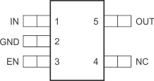
 Figure 5-1 TPS709: DBV Package,5-Pin SOT-23,Top View
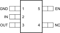
 Figure 5-3 TPS709B: DBV Package,5-Pin SOT-23,Top View
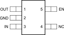
 Figure 5-2 TPS709A: DBV Package,5-Pin SOT-23,Top View
 Figure 5-4 DRV Package,6-Pin WSON,Top View
Table 5-1 Pin Functions
| PIN | I/O | DESCRIPTION | ||||
|---|---|---|---|---|---|---|
| NAME | DRV | DBV | ||||
| TPS709 | TPS709 | TPS709A | TPS709B | |||
| EN | 4 | 3 | 5 | 5 | I | Enable pin. Drive this pin high to enable the device. Drive this pin low to put the device into low current shutdown. This pin can be left floating to enable the device. The maximum voltage must remain below 6.5 V. |
| GND | 3 | 2 | 2 | 1 | — | Ground |
| IN | 6 | 1 | 3 | 2 | I | Unregulated input to the device |
| NC | 2, 5 | 4 | 4 | 4 | — | No internal connection |
| OUT | 1 | 5 | 1 | 3 | O | Regulated output voltage. Connect a small 2.2-µF or greater ceramic capacitor from this pin to ground to assure stability. |
| Thermal pad | — | — | — | — | The thermal pad is electrically connected to the GND node. Connect this pad to the GND plane for improved thermal performance. | |