SLVSBM4C September 2012 – January 2016 TPS717-Q1
PRODUCTION DATA.
- 1 Features
- 2 Applications
- 3 Description
- 4 Revision History
- 5 Pin Configuration and Functions
- 6 Specifications
- 7 Detailed Description
- 8 Application and Implementation
- 9 Power Supply Recommendations
- 10Layout
- 11Device and Documentation Support
- 12Mechanical, Packaging, and Orderable Information
封装选项
机械数据 (封装 | 引脚)
散热焊盘机械数据 (封装 | 引脚)
- DRV|6
订购信息
10 Layout
10.1 Layout Guidelines
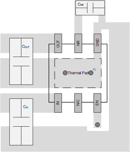
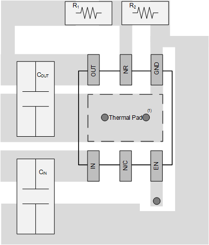
For best overall performance, place all circuit components on the same side of the circuit board and as near as practical to the respective LDO pin connections. Place ground return connections to the input and output capacitor, and to the LDO ground pin as close to the GND pin as possible, connected by wide, component-side, copper surface area. The use of vias and long traces to create LDO component connections is strongly discouraged and negatively affects system performance. This grounding and layout scheme minimizes inductive parasitics, and thereby reduces load-current transients, minimizes noise, and increases circuit stability. A ground reference plane is also recommended and is either embedded in the printed circuit board (PCB) itself or located on the bottom side of the PCB opposite the components. This reference plane serves to assure accuracy of the output voltage, shields the LDO from noise, and functions similar to a thermal plane to spread (or sink) heat from the LDO device when connected to the thermal pad. In most applications, this ground plane is necessary to meet thermal requirements.
10.1.1 Board Layout Recommendations to Improve PSRR and Noise Performance
To improve ac performance (such as PSRR, output noise, and transient response), TI recommends that the board be designed with separate ground planes for VIN and VOUT, with each ground plane connected only at the GND pin of the device. In addition, the ground connection for the bypass capacitor must connect directly to the GND pin of the device.
10.2 Layout Examples

