ZHCSAL2H February 2006 – January 2015 TPS717
PRODUCTION DATA.
- 1 特性
- 2 应用
- 3 说明
- 4 修订历史记录
- 5 Pin Configuration and Functions
- 6 Specifications
- 7 Detailed Description
- 8 Application and Implementation
- 9 Power Supply Recommendations
- 10Layout
- 11器件和文档支持
- 12机械封装和可订购信息
封装选项
机械数据 (封装 | 引脚)
散热焊盘机械数据 (封装 | 引脚)
- DRV|6
订购信息
10 Layout
10.1 Layout Guidelines
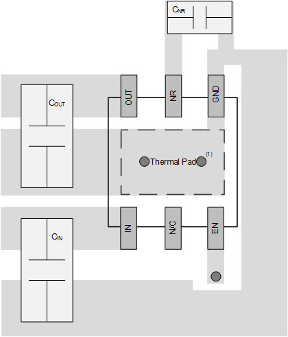
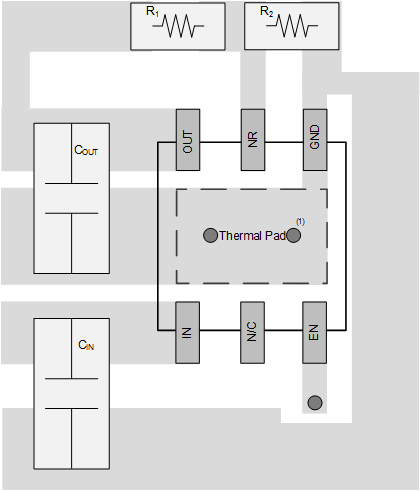
For best overall performance, place all circuit components on the same side of the circuit board and as near as practical to the respective LDO pin connections. Place ground return connections to the input and output capacitor, and to the LDO ground pin as close to the GND pin as possible, connected by wide, component-side, copper surface area. The use of vias and long traces to create LDO component connections is strongly discouraged and negatively affects system performance. This grounding and layout scheme minimizes inductive parasitics, and thereby reduces load-current transients, minimizes noise, and increases circuit stability. A ground reference plane is also recommended and is either embedded in the printed circuit board (PCB) itself or located on the bottom side of the PCB opposite the components. This reference plane serves to assure accuracy of the output voltage, shields the LDO from noise, and functions similar to a thermal plane to spread (or sink) heat from the LDO device when connected to the thermal pad. In most applications, this ground plane is necessary to meet thermal requirements.
10.1.1 Board Layout Recommendations to Improve PSRR and Noise Performance
To improve ac performance (such as PSRR, output noise, and transient response), TI recommends that the board be designed with separate ground planes for VIN and VOUT, with each ground plane connected only at the GND pin of the device. In addition, the ground connection for the bypass capacitor must connect directly to the GND pin of the device.
10.2 Layout Example


10.3 Power Dissipation
The ability to remove heat from the die is different for each package type, presenting different considerations in the printed circuit board (PCB) layout. The PCB area around the device that is free of other components moves the heat from the device to the ambient air. Performance data for JEDEC low- and high-K boards are given in Thermal Information. Using heavier copper increases the effectiveness in removing heat from the device. The addition of plated through-holes to heat-dissipating layers also improves the heatsink effectiveness.
Power dissipation depends on input voltage and load conditions. Power dissipation (PD) is equal to the product of the output current times the voltage drop across the output pass element (VIN to VOUT), as shown in Equation 4:

A better method of estimating the thermal measure comes from using the thermal metrics ΨJT and ΨJB, shown in Thermal Information. These metrics are a more accurate representation of the heat transfer characteristics of the die and the package than RθJA. The junction temperature can be estimated with Equation 5.

where
- PD is the power dissipation shown by Equation 4,
- TT is the temperature at the center-top of the IC package,
- TB is the PCB temperature measured 1 mm away from the IC package on the PCB surface.
NOTE
Both TT and TB can be measured on actual application boards using a thermo‐gun (an infrared thermometer).
For more information about measuring TT and TB, see the application note Using New Thermal Metrics (SBVA025), available for download at www.ti.com.