ZHCSAL2H February 2006 – January 2015 TPS717
PRODUCTION DATA.
- 1 特性
- 2 应用
- 3 说明
- 4 修订历史记录
- 5 Pin Configuration and Functions
- 6 Specifications
- 7 Detailed Description
- 8 Application and Implementation
- 9 Power Supply Recommendations
- 10Layout
- 11器件和文档支持
- 12机械封装和可订购信息
封装选项
机械数据 (封装 | 引脚)
散热焊盘机械数据 (封装 | 引脚)
- DRV|6
订购信息
6 Specifications
6.1 Absolute Maximum Ratings
over operating temperature range (unless otherwise noted), all voltages are with respect to GND(1)| MIN | MAX | UNIT | ||
|---|---|---|---|---|
| Voltage | VIN | –0.3 | 7 | V |
| VFB | –0.3 | 3.6 | V | |
| VNR | –0.3 | 3.6 | V | |
| VEN | –0.3 | VIN + 0.3 V(2) | V | |
| VOUT | –0.3 | 7 | V | |
| Current | IOUT | Internally limited | A | |
| Continuous total power dissipation | PDISS | See Thermal Information | ||
| Operating junction temperature | TJ | –55 | 150 | °C |
| Storage temperature | Tstg | –55 | 150 | °C |
(1) Stresses beyond those listed under Absolute Maximum Ratings may cause permanent damage to the device. These are stress ratings only, which do not imply functional operation of the device at these or any other conditions beyond those indicated under Recommended Operating Conditions. Exposure to absolute-maximum-rated conditions for extended periods may affect device reliability.
(2) VEN absolute maximum rating is VIN + 0.3 V or 7 V, whichever is greater.
6.2 ESD Ratings
| VALUE | UNIT | |||
|---|---|---|---|---|
| V(ESD) | Electrostatic discharge | Human body model (HBM), per ANSI/ESDA/JEDEC JS-001, all pins(1) | ±2000 | V |
| Charged device model (CDM), per JEDEC specification JESD22-C101, all pins(2) | ±500 | |||
(1) JEDEC document JEP155 states that 500-V HBM allows safe manufacturing with a standard ESD control process.
(2) JEDEC document JEP157 states that 250-V CDM allows safe manufacturing with a standard ESD control process.
6.3 Recommended Operating Conditions
over operating junction temperature range (unless otherwise noted)| MIN | NOM | MAX | UNIT | ||
|---|---|---|---|---|---|
| VIN | Input voltage | 2.5 | 6.5 | V | |
| VOUT | Output voltage | 0.9 | 5 | V | |
| IOUT | Output current | 0 | 150 | mA | |
| VEN | Enable voltage | 0 | VIN | V | |
| COUT | Output capacitor | 1 | 100 | µF | |
| TJ | Junction temperature | –40 | 125 | °C | |
6.4 Thermal Information
| THERMAL METRIC(1) | TPS717xx | UNIT | |||
|---|---|---|---|---|---|
| DCK | DRV | DSE | |||
| 5 PINS | 6 PINS | 6 PINS | |||
| RθJA | Junction-to-ambient thermal resistance | 279.2 | 71.1 | 190.5 | °C/W |
| RθJC(top) | Junction-to-case (top) thermal resistance | 57.5 | 96.5 | 94.9 | |
| RθJB | Junction-to-board thermal resistance | 74.1 | 40.5 | 149.3 | |
| ψJT | Junction-to-top characterization parameter | 0.8 | 2.7 | 6.4 | |
| ψJB | Junction-to-board characterization parameter | 73.1 | 40.9 | 152.8 | |
| RθJC(bot) | Junction-to-case (bottom) thermal resistance | n/a | 10.7 | n/a | |
(1) For more information about traditional and new thermal metrics, see the IC Package Thermal Metrics application report, SPRA953.
6.5 Electrical Characteristics
Over operating temperature range (TJ = –40°C to 125°C), VIN = VOUT(nom) + 0.5 V or 2.5 V, whichever is greater;IOUT = 0.5 mA, VEN = VIN, COUT = 1.0 μF, CNR = 0.01 μF, unless otherwise noted. For TPS71701, VOUT = 2.8 V.
Typical values are at TJ = 25°C.
| PARAMETER | TEST CONDITIONS | MIN | TYP | MAX | UNIT | |||
|---|---|---|---|---|---|---|---|---|
| VIN | Input voltage range(1) | 2.5 | 6.5 | V | ||||
| VFB | Internal reference (TPS71701) | 0.790 | 0.800 | 0.810 | V | |||
| VOUT | Output voltage range | (TPS717xx) | 0.9 | 5.0 | V | |||
| (TPS71701) | 0.9 | 6.5 – VDO | V | |||||
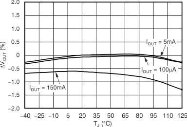
| VOUT | Output accuracy | Nominal | TJ = 25°C | ±2.5 | mV | |||
| Output accuracy (VOUT < 1.0 V) |
Over VIN, IOUT, Temp(3) | VOUT + 0.5 V ≤ VIN ≤ 6.5 V 0 mA ≤ IOUT ≤ 150 mA |
–30 | +30 | mV | |||
| Output accuracy
(VOUT ≥ 1.0 V) |
Over VIN, IOUT, Temp(3) | VOUT + 0.5 V ≤ VIN ≤ 6.5 V 0 mA ≤ IOUT ≤ 150 mA |
–3.0% | +3.0% | ||||
| ΔVOUT(ΔVIN) | Line regulation (1) | VOUT(nom) + 0.5 V ≤ VIN ≤ 6.5 V, IOUT = 5 mA |
125 | µV/V | ||||
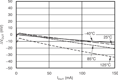
| ΔVOUT(ΔIOUT) | Load regulation | 0 mA ≤ IOUT ≤ 150 mA | 70 | µV/mA | ||||
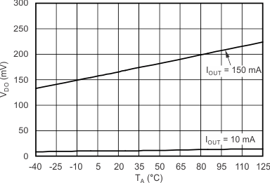
| VDO | Dropout voltage(2)
(VIN = VOUT(nom) – 0.1 V) |
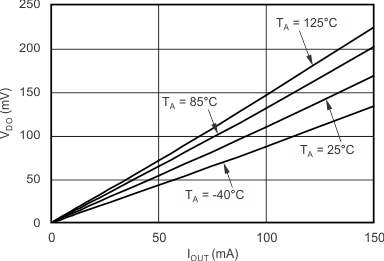
IOUT = 150 mA | 170 | 300 | mV | |||
| ILIM (fixed) | Output current limit (fixed output) | VOUT = 0.9 × VOUT(nom) | 200 | 325 | 575 | mA | ||
| ILIM (adjustable) | Output current limit (TPS71701) | VOUT = 0.9 × VOUT(nom) | 200 | 325 | 575 | mA | ||
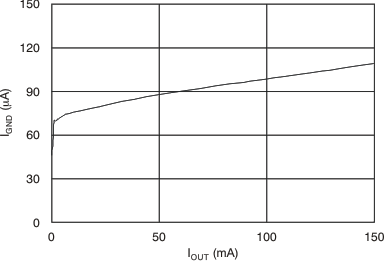
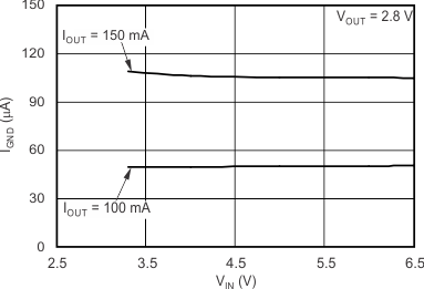
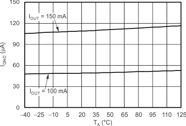
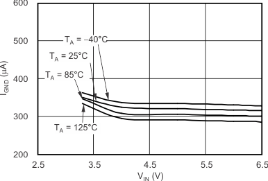
| IGND | Ground pin current | IOUT = 0.1 mA | 45 | 80 | μA | |||
| IOUT = 150 mA | 100 | μA | ||||||
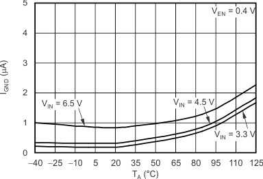
| ISHDN | Shutdown current (IGND) | VEN ≤ 0.4 V, TJ = –40°C to 85°C |
2.5 V ≤ VIN < 4.5 V | 0.20 | 1.5 | μA | ||
| 4.5 V ≤ VIN ≤ 6.5 V | 0.90 | μA | ||||||
| IFB | Feedback pin current (TPS71701) | 0.02 | 1.0 | μA | ||||
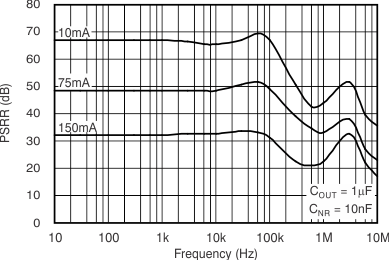
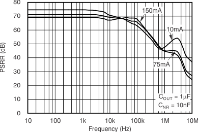
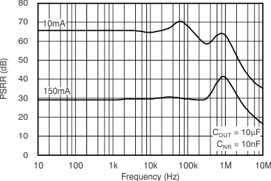
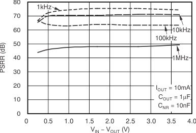
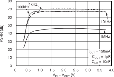
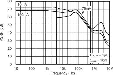
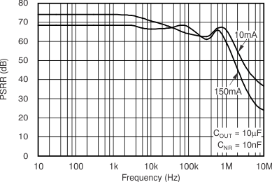
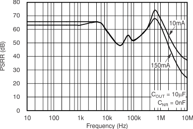
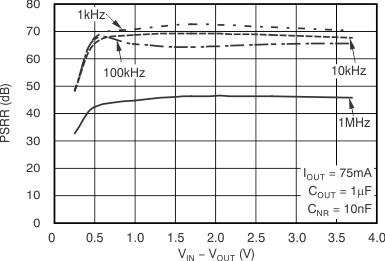
| PSRR | Power-supply rejection ratio | VIN = 3.8 V, VOUT = 2.8 V, IOUT = 150 mA |
f = 100 Hz | 70 | dB | |||
| f = 1 kHz | 70 | dB | ||||||
| f = 10 kHz | 67 | dB | ||||||
| f = 100 kHz | 67 | dB | ||||||
| f = 1 MHz | 45 | dB | ||||||
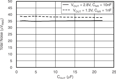
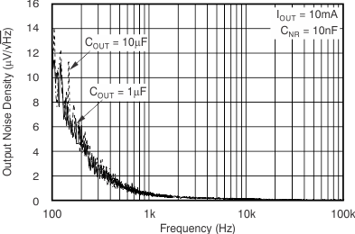
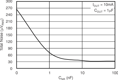
| Vn | Output noise voltage | BW = 100 Hz to 100 kHz, VIN = 3.8 V, VOUT = 2.8 V, IOUT = 10 mA |
CNR = none | 95 × VOUT | μVRMS | |||
| CNR = 0.001 μF | 25 × VOUT | μVRMS | ||||||
| CNR = 0.01 μF | 12.5 × VOUT | μVRMS | ||||||
| CNR = 0.1 μF | 11.5 × VOUT | μVRMS | ||||||
| tSTR | Startup time | VOUT = 90% VOUT(nom), RL = 19 Ω, COUT = 1 μF |
0.9 V ≤ VOUT ≤ 1.6V, CNR = 0.001 μF | 0.700 | ms | |||
| 1.6 V < VOUT < VMAX, CNR = 0.01 μF | 0.160 | ms | ||||||
| VEN(high) | Enable high (enabled) | VIN ≤ 5.5 V | 1.2 | 6.5(4) | V | |||
| 5.5 V < VIN ≤ 6.5 V | 1.25 | 6.5 | V | |||||
| VEN(low) | Enable low (shutdown) | 0 | 0.4 | V | ||||
| IEN(high) | Enable pin current, enabled | EN = 6.5 V | 0.02 | 1.0 | μA | |||
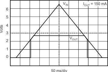
| UVLO | Undervoltage lockout | VIN rising | 2.41 | 2.45 | 2.49 | V | ||
| Hysteresis | VIN falling | 150 | mV | |||||
| Tsd | Thermal shutdown temperature | Shutdown, temperature increasing | 160 | °C | ||||
| Reset, temperature decreasing | 140 | °C | ||||||
| TJ | Operating junction temperature | –40 | 125 | °C | ||||
(1) Minimum VIN = VOUT + VDO or 2.5 V, whichever is greater.
(2) VDO is not measured for devices with VOUT(nom) < 2.6 V because the minimum VINis 2.5 V.
(3) Does not include external resistor tolerances.
(4) Maximum VEN(high) = VIN + 0.3 or 6.5 V, whichever is smaller.
6.6 Typical Characteristics
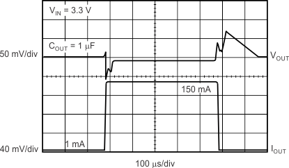
Over operating temperature range (TJ = –40°C to 125°C), VIN = VOUT(nom) + 0.5 V or 2.5 V, whichever is greater; IOUT = 0.5 mA, VEN = VIN, COUT = 1 μF, CNR = 0.01 μF, unless otherwise noted. For the adjustable version (TPS71701,) VOUT = 2.8 V. Typical values are at TA = 25°C.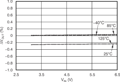
Output Capacitance
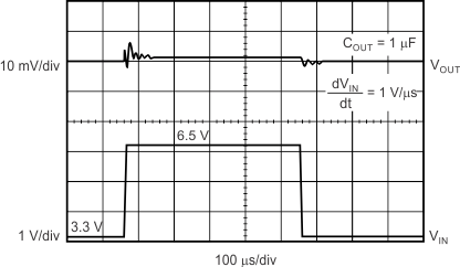
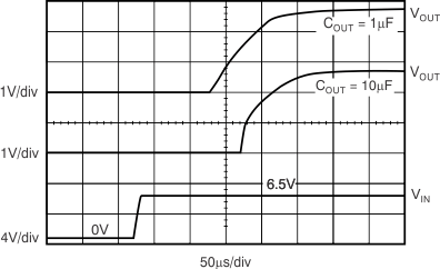
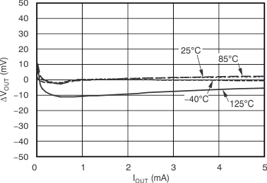
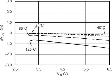
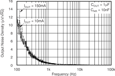
Output Current
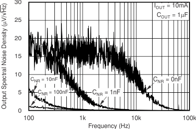
Noise Reduction
