ZHCSAL2H February 2006 – January 2015 TPS717
PRODUCTION DATA.
- 1 特性
- 2 应用
- 3 说明
- 4 修订历史记录
- 5 Pin Configuration and Functions
- 6 Specifications
- 7 Detailed Description
- 8 Application and Implementation
- 9 Power Supply Recommendations
- 10Layout
- 11器件和文档支持
- 12机械封装和可订购信息
封装选项
机械数据 (封装 | 引脚)
散热焊盘机械数据 (封装 | 引脚)
- DRV|6
订购信息
7 Detailed Description
7.1 Overview
The TPS717xx family of low-dropout (LDO) regulators combines the high performance required by many RF and precision analog applications with ultra-low current consumption. High PSRR is provided by a high-gain, high-bandwidth error loop with good supply rejection with very low headroom (VIN – VOUT). Fixed voltage versions provide a noise reduction pin to bypass noise generated by the band-gap reference and to improve PSRR. A quick-start circuit fast-charges this capacitor at startup. The combination of high performance and low ground current also make the TPS717xx family of devices an excellent choice for battery-powered applications. All versions have thermal and overcurrent protection.
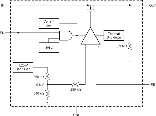
7.2 Functional Block Diagrams
 Figure 32. Adjustable Voltage Version
7.3 Feature Description
7.3.1 Internal Current Limit
The TPS717xx internal current limit helps protect the regulator during fault conditions. During current limit, the output sources a fixed amount of current that is largely independent of output voltage. For reliable operation, do not operate the device in a current-limit state for extended periods of time.
The PMOS pass element in the TPS717xx has a built-in body diode that conducts current when the voltage at OUT exceeds the voltage at IN. This current is not limited, so if extended reverse voltage operation is anticipated, external limiting may be appropriate.
7.3.2 Shutdown
The enable pin (EN) is active high and compatible with standard and low voltage, TTL-CMOS levels. When shutdown capability is not required, EN can be connected to IN.
7.3.3 Startup and Noise Reduction Capacitor
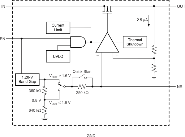
Fixed voltage versions of the TPS717xx use a quick-start circuit to fast-charge the noise reduction capacitor, CNR, if present (see Figure 31). This circuit allows the combination of very low output noise and fast start-up times. The NR pin is high impedance, so a low-leakage CNR capacitor must be used; most ceramic capacitors are appropriate in this configuration.
Note that for fastest startup, apply VIN first, then the enable pin (EN) driven high. If EN is tied to IN, startup is somewhat slower. Refer to Figure 29 in Typical Characteristics. The quick-start switch is closed for approximately 135 μs. To ensure that CNR is fully charged during the quick-start time, use a 0.01-μF or smaller capacitor.
For output voltages below 1.6 V, a voltage divider on the band-gap reference voltage is employed to optimize output regulation performance for lower output voltages. This configuration results in an additional resistor in the quick-start path and combined with the noise reduction capacitor (CNR) results in slower start-up times for output voltages below 1.6 V.
Equation 1 approximates the start-up time as a function of CNR for output voltages below 1.6 V:

7.3.4 Undervoltage Lockout (UVLO)
The TPS717xx uses an undervoltage lockout circuit to keep the output shut off until the internal circuitry is operating properly. The UVLO circuit has a limited glitch immunity so undershoot transients are typically ignored on the input if these transients are less than 5 μs in duration.
7.3.5 Minimum Load
The TPS717xx is stable with no output load. Traditional PMOS LDO regulators suffer from lower loop gain at very light output loads. The TPS717xx employs an innovative low-current mode circuit to increase loop gain under very light or no-load conditions, resulting in improved output voltage regulation performance down to zero output current.
7.3.6 Thermal Protection
Thermal protection disables the output when the junction temperature rises to approximately 160°C, allowing the device to cool. When the junction temperature cools to approximately 140°C the output circuitry is again enabled. Depending on power dissipation, thermal resistance, and ambient temperature, the thermal protection circuit can cycle on and off. This cycling limits the dissipation of the regulator, protecting it from damage because of overheating.
Any tendency to activate the thermal protection circuit indicates excessive power dissipation or an inadequate heatsink. For reliable operation, limit junction temperature to 125°C maximum. To estimate the margin of safety in a complete design (including heatsink), increase the ambient temperature until the thermal protection is triggered; use worst-case loads and signal conditions. For good reliability, trigger thermal protection at least 35°C above the maximum expected ambient condition of a particular application. This configuration produces a worst-case junction temperature of 125°C at the highest expected ambient temperature and worst-case load.
The internal protection circuitry of the TPS717xx is designed to protect against overload conditions. This circuitry is not intended to replace proper heatsinking. Continuously running the TPS717xx into thermal shutdown degrades device reliability.
7.4 Device Functional Modes
7.4.1 Normal Operation
The device regulates to the nominal output voltage under the following conditions:
- The input voltage has previously exceeded the UVLO rising voltage and has not decreased below the UVLO falling threshold.
- The input voltage is greater than the nominal output voltage added to the dropout voltage.
- The enable voltage has previously exceeded the enable rising threshold voltage and has not decreased below the enable falling threshold.
- The output current is less than the current limit.
- The device junction temperature is less than the maximum specified junction temperature.
7.4.2 Dropout Operation
If the input voltage is lower than the nominal output voltage plus the specified dropout voltage, but all other conditions are met for normal operation, the device operates in dropout mode. In this condition, the output voltage is the same as the input voltage minus the dropout voltage. The transient performance of the device is significantly degraded because the pass device is in a triode state and no longer controls the current through the LDO. Line or load transients in dropout can result in large output voltage deviations.
7.4.3 Disabled
The device is disabled under the following conditions:
- The input voltage is less than the UVLO falling voltage, or has not yet exceeded the UVLO rising threshold.
- The enable voltage is less than the enable falling threshold voltage or has not yet exceeded the enable rising threshold.
- The device junction temperature is greater than the thermal shutdown temperature.
Table 1 shows the conditions that lead to the different modes of operation.
Table 1. Device Functional Mode Comparison
| OPERATING MODE | PARAMETER | |||
|---|---|---|---|---|
| VIN | VEN | IOUT | TJ | |
| Normal mode | VIN > VOUT(nom) + VDO and VIN > UVLO | VEN > VEN(high) | I OUT < ILIM | T J < 125°C |
| Dropout mode | UVLO < VIN < VOUT(nom) + VDO | VEN > VEN(high) | — | TJ < 125°C |
| Disabled mode (any true condition disables the device) |
VIN < UVLO – Vhys | VEN < VEN(low) | — | TJ > 165°C |
