ZHCSEN1A February 2016 – October 2016 TPS720-Q1
PRODUCTION DATA.
8 Application and Implementation
NOTE
Information in the following applications sections is not part of the TI component specification, and TI does not warrant its accuracy or completeness. TI’s customers are responsible for determining suitability of components for their purposes. Customers should validate and test their design implementation to confirm system functionality.
8.1 Application Information
8.1.1 Input and Output Capacitor Requirements
Although a capacitor is not required for stability on the IN pin, good analog design practice is to connect a 0.1-μF to 1-μF low equivalent series resistance (ESR) capacitor across the IN pin input supply near the regulator. This capacitor counteracts reactive input sources and improves transient response, noise rejection, and ripple rejection. A higher-value capacitor may be necessary if large, fast rise-time load transients are anticipated, or if the device is located far from the power source. If source impedance is not sufficiently low, a 0.1-μF input capacitor may be necessary to ensure stability.
The BIAS pin does not require an input capacitor because BIAS does not source high currents. However, if source impedance is not sufficiently low, TI recommends a small 0.1-µF bypass capacitor.
The TPS720-Q1 is designed to be stable with standard ceramic capacitors with values of 2.2 μF or larger at the output. X5R- and X7R-type capacitors are best because they have minimal variation in value and ESR over temperature. Maximum ESR must be less than 250 mΩ.
8.1.2 Output Regulation With the IN Pin Floating
The TPS720-Q1 supports a novel feature where the output of the LDO regulates under light loads when the IN pin is left floating. Under normal conditions when the IN pin is connected to a power source, the BIAS pin draws only tens of milliamperes. However, when the IN pin is floating, an innovative circuit allows a maximum current of 500 μA to be drawn by the load through the BIAS pin and maintains the output in regulation. This feature is particularly useful in power-saving applications where a dc-dc converter connected to the IN pin is disabled, but the LDO is required to regulate the output voltage to a light load.
Figure 25 shows an application example where a microcontroller is not turned off (to maintain the state of the internal memory), but where the regulated supply (shown as the TPS62xxx) is turned off to reduce power. In this case, the TPS720-Q1 BIAS pin provides sufficient load current to maintain a regulated voltage to the microcontroller.
 Figure 25. Floating IN Pin Regulation Example
8.1.3 Dropout Voltage
The TPS720-Q1 uses a NMOS pass transistor to achieve low dropout. When (VIN – VOUT) is less than the dropout voltage (VDO), the NMOS pass device is in the linear region of operation and the input-to-output resistance is the RDS(ON) of the NMOS pass element. VDO approximately scales with output current because the NMOS device behaves like a resistor in dropout.
PSRR and transient response are degraded when (VIN – VOUT) approaches dropout. This effect is shown in Figure 19.
8.1.4 Transient Response
Increasing the size of the output capacitor reduces overshoot and undershoot magnitude but increases duration of the transient response.
8.1.5 Minimum Load
The TPS720-Q1 is stable with no output load. Although some LDOs suffer from low loop gain at very light output loads, the TPS720-Q1 employs an innovative, low-current mode circuit under very light or no-load conditions which improves output voltage regulation performance.
8.2 Typical Application
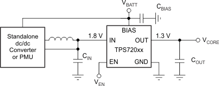
 Figure 26. Typical Application Schematic
8.2.1 Design Requirements
Table 1 lists the parameters for this design example.
Table 1. Design Parameters
| DESIGN PARAMETER | EXAMPLE VALUE |
|---|---|
| VIN | 2.3 V |
| VBIAS | 3.2 V |
| VOUT | 1.8 V |
| IOUT | 10-mA typical, 350-mA peak |
8.2.2 Detailed Design Procedures
TI recommends selecting the minimum component size; a small size solution for this design example is desired. Set CIN = 1 µF, C BIAS = 100 nF, and COUT = 2.2 µF.
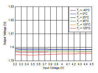
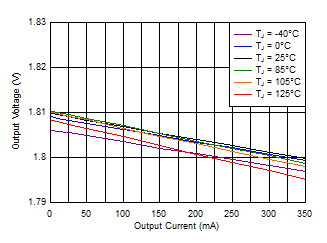
8.2.3 Application Curves

| IOUT = 350 mA |
