SBVS128F June 2009 – December 2015 TPS727
PRODUCTION DATA.
- 1 Features
- 2 Applications
- 3 Description
- 4 Revision History
- 5 Pin Configurations and Functions
- 6 Specifications
- 7 Detailed Description
- 8 Applications and Implementation
- 9 Power-Supply Recommendations
- 10Layout
- 11Device and Documentation Support
- 12Mechanical, Packaging, and Orderable Information
封装选项
请参考 PDF 数据表获取器件具体的封装图。
机械数据 (封装 | 引脚)
- YFF|4
- DSE|6
散热焊盘机械数据 (封装 | 引脚)
订购信息
7 Detailed Description
7.1 Overview
The TPS727 devices belong to a family of LDO regulators that consume extremely low quiescent current while simultaneously delivering excellent PSRR with very little headroom (VIN – VOUT differential voltage), and very good transient response. These features, combined with low noise without a noise reduction pin in an ultrasmall package, make these devices ideal for portable applications. This family of regulators offers sub-band-gap output voltages, current limit and thermal protection, and is fully specified from –40°C to +125°C.
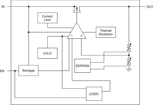
7.2 Functional Block Diagram

7.3 Feature Description
7.3.1 Internal Current Limit
The TPS727 internal current limit helps protect the regulator during fault conditions. During current limit, the output sources a fixed amount of current that is largely independent of output voltage. In such a case, the output voltage is not regulated and is VOUT = ILIMIT × RLOAD. The PMOS pass transistor dissipates (VIN – VOUT) × ILIMIT until thermal shutdown is triggered and the device is turned off. As the device cools down, it is turned on by the internal thermal shutdown circuit. If the fault condition continues, the device cycles between current limit and thermal shutdown. See the Thermal Protection section for more details.
The PMOS pass element in the TPS727 has a built-in body diode that conducts current when the voltage at the OUT pin exceeds the voltage at the IN pin. This current is not limited, so if extended reverse voltage operation is anticipated, external limiting to 5% of rated output current is recommended.
7.3.2 Soft Start
The startup current is given by Equation 1:

Equation 1 shows that soft-start current is directly proportional to COUT.
The output voltage ramp rate is independent of COUT and load current, and has a typical value of 0.07 V/μs.
The TPS727 automatically adjusts the soft-start current to supply both the load current and the COUT charge current. For example, if ILOAD = 0 mA upon enabling the LDO, ISOFT START = 1 μF × 0.07 V/μs + 0 mA = 70 mA, the current that charges the output capacitor.
If ILOAD = 200 mA, ISOFT START = 1 μF × 0.07 V/μs + 200 mA = 270 mA, the current required for charging output capacitor and supplying the load current.
If the output capacitor and load are increased such that the soft-start current exceeds the output current limit, the current is clamped at the typical current limit of 400 mA. For example, if COUT = 10 μF and IOUT = 200 mA, 10 μF × 0.07 V/μs + 200 mA = 900 mA is not supplied. Instead, the current is clamped at 400 mA.
7.3.3 Shutdown
The enable pin (EN) is active high and is compatible with standard and low voltage, TTL-CMOS levels. When shutdown capability is not required, EN can be connected to the IN pin.
7.3.4 Dropout Voltage
The TPS727 uses a PMOS pass transistor to achieve low dropout. When (VIN – VOUT) is less than the dropout voltage (VDO), the PMOS pass device is in the linear region of operation and the input-to-output resistance is the RDS(ON) of the PMOS pass element. VDO approximately scales with output current because the PMOS device functions like a resistor in dropout.
As with any linear regulator, PSRR and transient response are degraded as (VIN – VOUT) approaches dropout. This effect is illustrated in Figure 15 in the Typical Characteristics section.
7.3.5 Undervoltage Lock-out (UVLO)
The TPS727 uses an undervoltage lock-out circuit that keeps the output shut off until the input voltage reaches the UVLO threshold voltage.
7.3.6 Thermal Protection
Thermal protection disables the output when the junction temperature rises to approximately +160°C, allowing the device to cool. When the junction temperature cools to approximately +140°C the output circuitry is again enabled. Depending on power dissipation, thermal resistance, and ambient temperature, the thermal protection circuit may cycle on and off. This cycling limits the dissipation of the regulator, protecting it from damage as a result of overheating.
Any tendency to activate the thermal protection circuit indicates excessive power dissipation or an inadequate heatsink. For reliable operation, limit junction temperature to +125°C maximum. To estimate the margin of safety in a complete design (including heatsink), increase the ambient temperature until the thermal protection is triggered; use worst-case loads and signal conditions. For good reliability, thermal protection triggers at least +35°C above the maximum expected ambient condition of a particular application. This configuration produces a worst-case junction temperature of +125°C at the highest expected ambient temperature and worst-case load.
The internal protection circuitry of the TPS727 is designed to protect against overload conditions. This circuitry is not intended to replace proper heatsinking. Continuously running the TPS727 into thermal shutdown degrades device reliability.
7.4 Device Functional Modes
7.4.1 Operation with EN Control
Driving EN over 0.9 V turns on the regulator. Driving EN below 0.4 V puts the regulator into shutdown mode, thus reducing the operating current to 120 nA, nominal.