SBVS054J November 2004 – April 2015 TPS730
PRODUCTION DATA.
- 1 Features
- 2 Applications
- 3 Description
- 4 Revision History
- 5 Pin Configuration and Functions
- 6 Specifications
- 7 Detailed Description
- 8 Application and Implementation
- 9 Power Supply Recommendations
- 10Layout
- 11Device and Documentation Support
- 12Mechanical, Packaging, and Orderable Information
7 Detailed Description
7.1 Overview
The TPS730 family of low-dropout (LDO) regulators has been optimized for use in noise-sensitive, battery-operated equipment. The device features extremely low dropout voltages, high PSRR, ultra-low output noise, low quiescent current (170 μA typically), and enable-input to reduce supply currents to less than 1 μA when the regulator is turned off.
7.2 Functional Block Diagrams
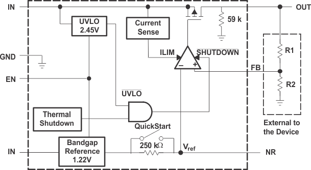
 Figure 15. TPS730 Block Diagram (Adjustable-Voltage Version)
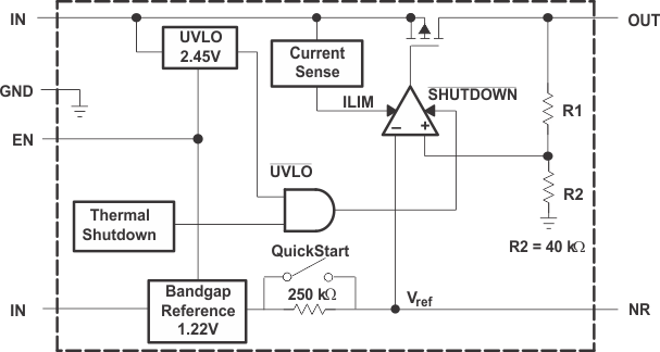
 Figure 16. TPS730 Block Diagram (Fixed-Voltage Versions)
7.3 Feature Description
7.3.1 Undervoltage Lockout (UVLO)
The TPS730 uses an undervoltage lockout (UVLO) circuit that disables the output until the input voltage is greater than the rising UVLO voltage. This circuit ensures that the device does not exhibit any unpredictable behavior when the supply voltage is lower than the operational range of the internal circuitry, VIN(min).
7.3.2 Shutdown
The enable pin (EN) is active high. Enable the device by forcing the EN pin to exceed VEN(high) (1.7 V, minimum). Turn off the device by forcing the EN pin to drop below 0.7 V. If shutdown capability is not required, connect EN to IN.
7.3.3 Foldback Current Limit
The TPS730 features internal current limiting and thermal protection. During normal operation, the TPS730 limits output current to approximately 400 mA. When current limiting engages, the output voltage scales back linearly until the overcurrent condition ends. While current limiting is designed to prevent gross device failure, do not exceed the power dissipation ratings of the package or the absolute maximum voltage ratings of the device.
7.4 Device Functional Modes
7.4.1 Normal Operation
The device regulates to the nominal output voltage under the following conditions:
- The input voltage is at least as high as VIN(min).
- The input voltage is greater than the nominal output voltage added to the dropout voltage.
- The enable voltage is greater than VEN(min).
- The output current is less than the current limit.
- The device junction temperature is less than the maximum specified junction temperature.
7.4.2 Dropout Operation
If the input voltage is lower than the nominal output voltage plus the specified dropout voltage, but all other conditions are met for normal operation, the device operates in dropout mode. In this mode of operation, the output voltage is the same as the input voltage minus the dropout voltage. The transient performance of the device is significantly degraded because the pass device is in the linear region and no longer controls the current through the LDO. Line or load transients in dropout can result in large output voltage deviations.
7.4.3 Disabled
The device is disabled under the following conditions:
- The enable voltage is less than the enable falling threshold voltage or has not yet exceeded the enable rising threshold.
- The device junction temperature is greater than the thermal shutdown temperature.
- The input voltage is less than UVLOfalling.
Table 1 shows the conditions that lead to the different modes of operation.
Table 1. Device Functional Mode Comparison
| OPERATING MODE | PARAMETER | |||
|---|---|---|---|---|
| VIN | VEN | IOUT | TJ | |
| Normal mode | VIN > VOUT(nom) + VDO and VIN > VIN(min) |
VEN > VEN(high) | IOUT < ILIM | TJ < 125°C |
| Dropout mode | VIN(min) < VIN < VOUT(nom) + VDO | VEN > VEN(high) | — | TJ < 125°C |
| Disabled mode (any true condition disables the device) |
VIN < UVLOfalling | VEN < VEN(low) | — | TJ > 165°C(1) |