ZHCSIE2M June   2008  – June 2018 TPS735

PRODUCTION DATA.  

  1. 特性
  2. 应用
  3. 说明
    1.     典型应用
  4. 修订历史记录
    1.     Pin Configuration and Functions
      1.      Pin Functions
  5. Specifications
    1. 5.1 Absolute Maximum Ratings
    2. 5.2 ESD Ratings
    3. 5.3 Recommended Operating Conditions
    4. 5.4 Thermal Information
    5. 5.5 Electrical Characteristics
    6. 5.6 Typical Characteristics
  6. Detailed Description
    1. 6.1 Overview
    2. 6.2 Functional Block Diagrams
    3. 6.3 Feature Description
      1. 6.3.1 Internal Current Limit
      2. 6.3.2 Shutdown
      3. 6.3.3 Dropout Voltage
      4. 6.3.4 Start-Up and Noise Reduction Capacitor
      5. 6.3.5 Transient Response
      6. 6.3.6 Undervoltage Lockout
      7. 6.3.7 Minimum Load
      8. 6.3.8 Thermal Protection
    4. 6.4 Device Functional Modes
      1. 6.4.1 Normal Operation
      2. 6.4.2 Dropout Operation
      3. 6.4.3 Disabled
  7. Application and Implementation
    1. 7.1 Application Information
    2. 7.2 Typical Applications
      1. 7.2.1 Design Requirements
        1. 7.2.1.1 Input and Output Capacitor Requirements
        2. 7.2.1.2 Feed-Forward Capacitor Requirements
      2. 7.2.2 Detailed Design Procedure
        1. 7.2.2.1 Output Noise
      3. 7.2.3 Application Curves
  8. Power Supply Recommendations
  9. Layout
    1. 9.1 Layout Guidelines
      1. 9.1.1 Board Layout Recommendations to Improve PSRR and Noise Performance
    2. 9.2 Layout Example
    3. 9.3 Power Dissipation
    4. 9.4 Estimating Junction Temperature
    5. 9.5 Package Mounting
  10. 10器件和文档支持
    1. 10.1 器件支持
      1. 10.1.1 开发支持
        1. 10.1.1.1 评估模块
      2. 10.1.2 器件命名规则
    2. 10.2 文档支持
      1. 10.2.1 相关文档
    3. 10.3 商标
    4. 10.4 静电放电警告
    5. 10.5 术语表
  11. 11机械、封装和可订购信息

封装选项

机械数据 (封装 | 引脚)
散热焊盘机械数据 (封装 | 引脚)
订购信息

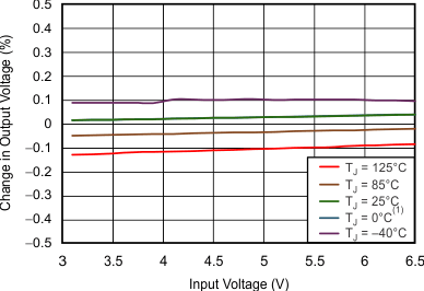
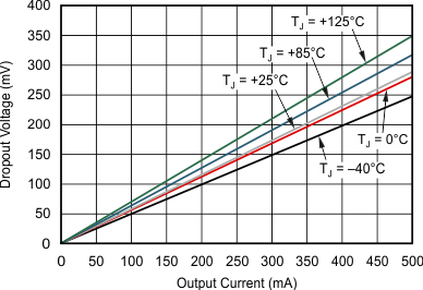
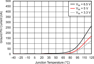
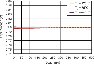
Typical Characteristics

over operating temperature range (TJ= –40°C to +125°C), VIN = VOUT(nom) + 0.5 V or 2.7 V, whichever is greater; IOUT = 1 mA, VEN = VIN,COUT = 2.2 μF, CNR = 10 nF. Typical values are at TJ = 25°C, (unless otherwise noted).
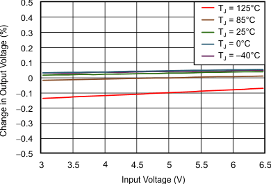
TPS735 tc_line_reg_73501_sbvs252.gif
Results for TJ = 0°C are similar to TJ = 25°C.
IOUT = 100 mA
Figure 1. TPS735 Line Regulation
TPS735 tc_load_reg_73501_sbvs252.gif
The y-axis range is ±2% of 2.8 V
Figure 3. TPS735 Load Regulation
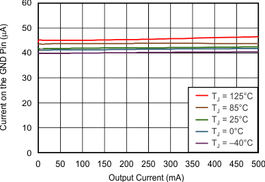
TPS735 tc_ignd_iout_sbvs252.gif
Figure 5. TPS735 Ground Pin Current vs
Output Current
TPS735 tc_dropout_volt_vs_output_current_bvs087.gif
VEN = 0.4 V
Figure 7. TPS735 Dropout Voltage vs Output Current
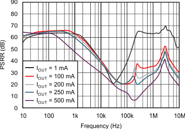
TPS735 tc_psrr_fqcy_05v_sbvs252.gif
(VIN – VOUT = 0.5 V)
Figure 9. Power-Supply Ripple Rejection vs Frequency
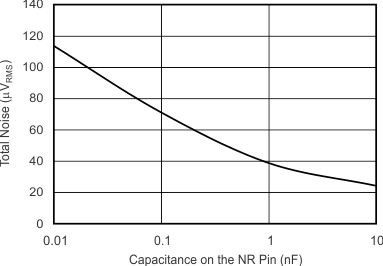
TPS735 tc_noise_cnr_sbvs252.gif
Figure 11. TPS73525 RMS Noise vs CNR
TPS735 tc_line_reg_73525_sbvs252.gif
IOUT = 100 mA
Figure 2. TPS735 Line Regulation
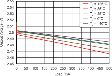
TPS735 tc_load_reg_73525_sbvs252.gif
The y-axis range is ±2% of 2.5 V
Figure 4. TPS735 Load Regulation
TPS735 tc_ignd_disable_temp_sbvs252.gif
Figure 6. TPS735 Ground Pin Current (Disable) vs Temperature
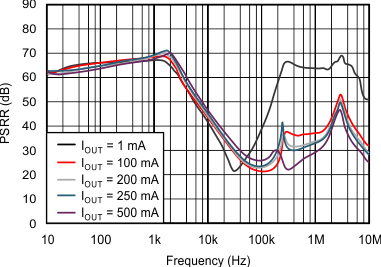
TPS735 tc_psrr_fqcy_1v_sbvs252.gif
(VIN – VOUT = 1 V)
Figure 8. Power-Supply Ripple Rejection vs Frequency
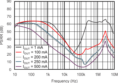
TPS735 tc_psrr_fqcy_03v_sbvs252.gif
(VIN – VOUT = 0.3 V)
Figure 10. Power-Supply Ripple Rejection vs Frequency
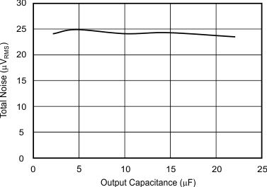
TPS735 tc_noise_cout_sbvs252.gif
CNR = 0.01 µF, IOUT = 1 mA
Figure 12. TPS735 RMS Noise vs COUT