ZHCSUK3O December 2005 – October 2024 TPS74201
PRODUCTION DATA
- 1
- 1 特性
- 2 应用
- 3 说明
- 4 Pin Configuration and Functions
- 5 Specifications
- 6 Detailed Description
- 7 Application and Implementation
- 8 Device and Documentation Support
- 9 Revision History
- 10Mechanical, Packaging, and Orderable Information
封装选项
机械数据 (封装 | 引脚)
散热焊盘机械数据 (封装 | 引脚)
订购信息
7.2 Typical Applications
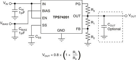
Figure 7-4 is a typical application circuit for the TPS742 adjustable output device.
R1 and R2 can be calculated for any output voltage using the formula shown in Figure 7-4. See Table 7-2 for sample resistor values of common output voltages. To achieve the maximum accuracy specifications, R2 must be ≤ 4.99 kΩ.
 Figure 7-4 Typical Application Circuit for the TPS742
Table 7-2 Standard 1% Resistor Values for Programming the Output Voltage
(See Equation 5)
(See Equation 5)
| R1 (kΩ) | R2 (kΩ) | VOUT (V) |
|---|---|---|
| Short | Open | 0.8 |
| 0.619 | 4.99 | 0.9 |
| 1.13 | 4.53 | 1 |
| 1.37 | 4.42 | 1.05 |
| 1.87 | 4.99 | 1.1 |
| 2.49 | 4.99 | 1.2 |
| 4.12 | 4.75 | 1.5 |
| 3.57 | 2.87 | 1.8 |
| 3.57 | 1.69 | 2.5 |
| 3.57 | 1.15 | 3.3 |
Equation 5. VOUT = 0.8 × (1 + R1/R2)
Note:
When VBIAS and VEN are present and VIN is not supplied, this device outputs approximately 50 μA of current from OUT. Although this condition does not cause any damage to the device, the output current can charge up the OUT node if total resistance between OUT and GND (including external feedback resistors) is greater than 10 kΩ.