ZHCSUK3O December 2005 – October 2024 TPS74201
PRODUCTION DATA
- 1
- 1 特性
- 2 应用
- 3 说明
- 4 Pin Configuration and Functions
- 5 Specifications
- 6 Detailed Description
- 7 Application and Implementation
- 8 Device and Documentation Support
- 9 Revision History
- 10Mechanical, Packaging, and Orderable Information
封装选项
机械数据 (封装 | 引脚)
散热焊盘机械数据 (封装 | 引脚)
订购信息
5.6 Typical Characteristics
at TJ = 25°C, VOUT = 1.5V, VIN = VOUT(NOM) + 0.3V, VBIAS = 3.3V (legacy chip), VBIAS = 5.0V (new chip), IOUT = 50 mA, VEN =VIN, CIN = 1μF, CBIAS = 4.7μF, CSS = 0.01μF (legacy chip), and COUT = 10μF (unless otherwise noted)
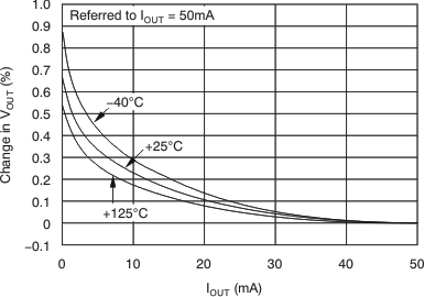
| Legacy chip |
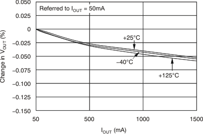 Figure 5-3 Load Regulation
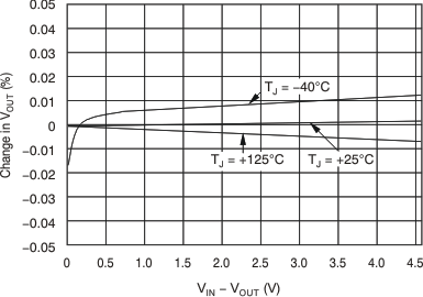 Figure 5-5 Line Regulation
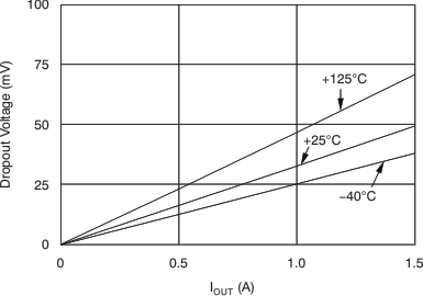 Figure 5-7 VIN Dropout Voltage vs IOUT and Temperature (TJ)
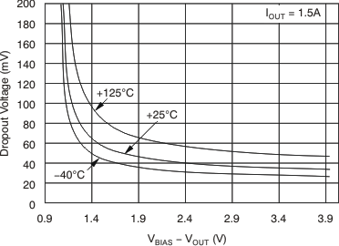 Figure 5-9 VIN Dropout Voltage vs VBIAS – VOUT and Temperature (TJ)
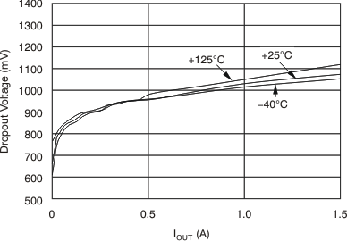 Figure 5-11 VBIAS Dropout Voltage vs IOUT and Temperature
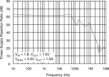 Figure 5-13 VBIAS PSRR vs Frequency
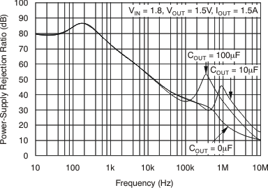 Figure 5-15 VIN PSRR vs Frequency
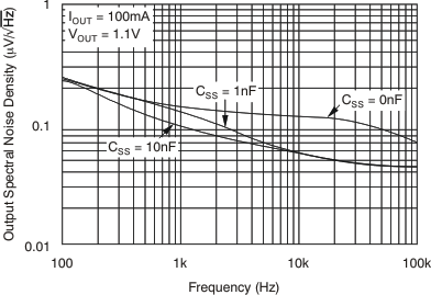 Figure 5-17 Noise Spectral Density
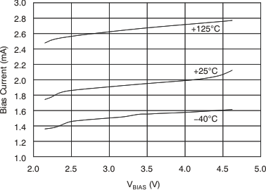 Figure 5-19 IBIAS vs VBIAS and VOUT
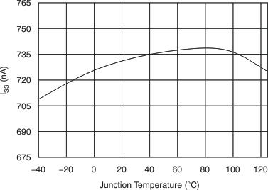 Figure 5-21 Soft-Start Charging Current (ISS) vs Temperature
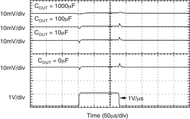
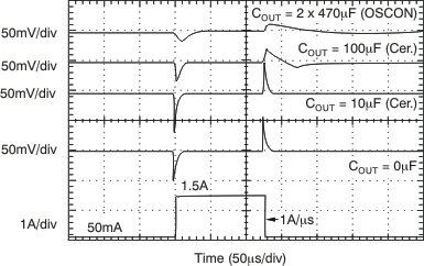 Figure 5-25 Output Load Transient Response
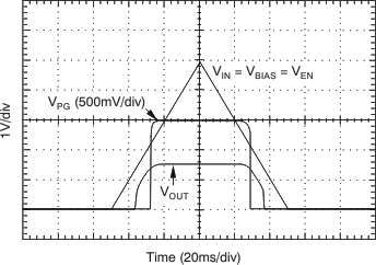 Figure 5-27 Power Up and Power Down
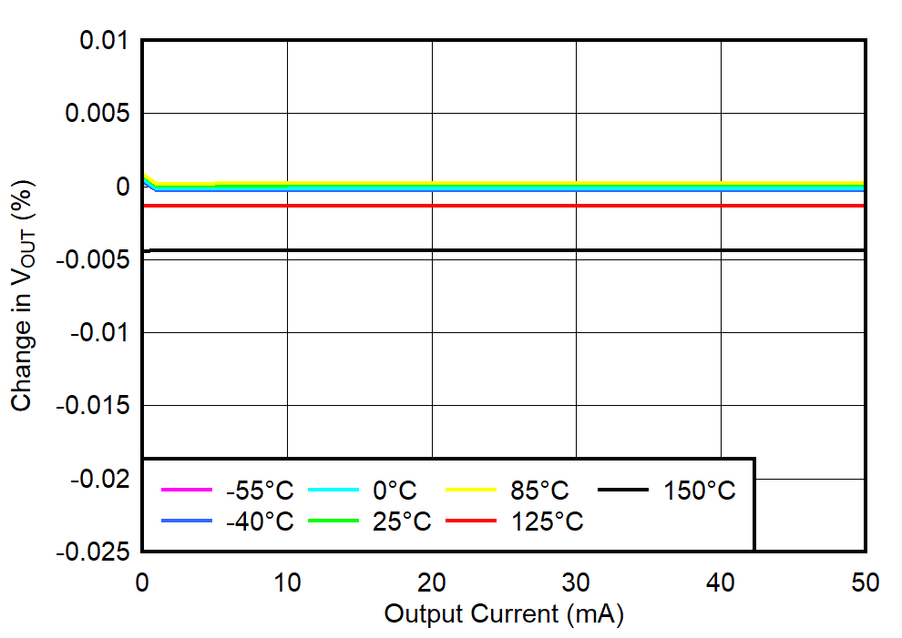 Figure 5-2 Load Regulation
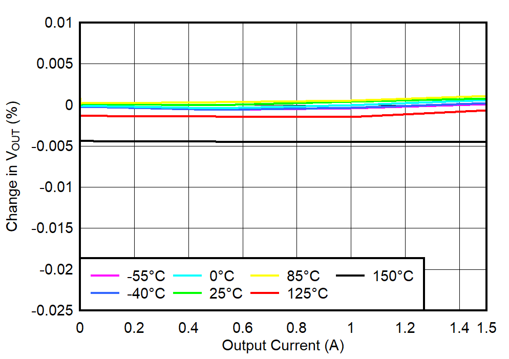 Figure 5-4 Load Regulation
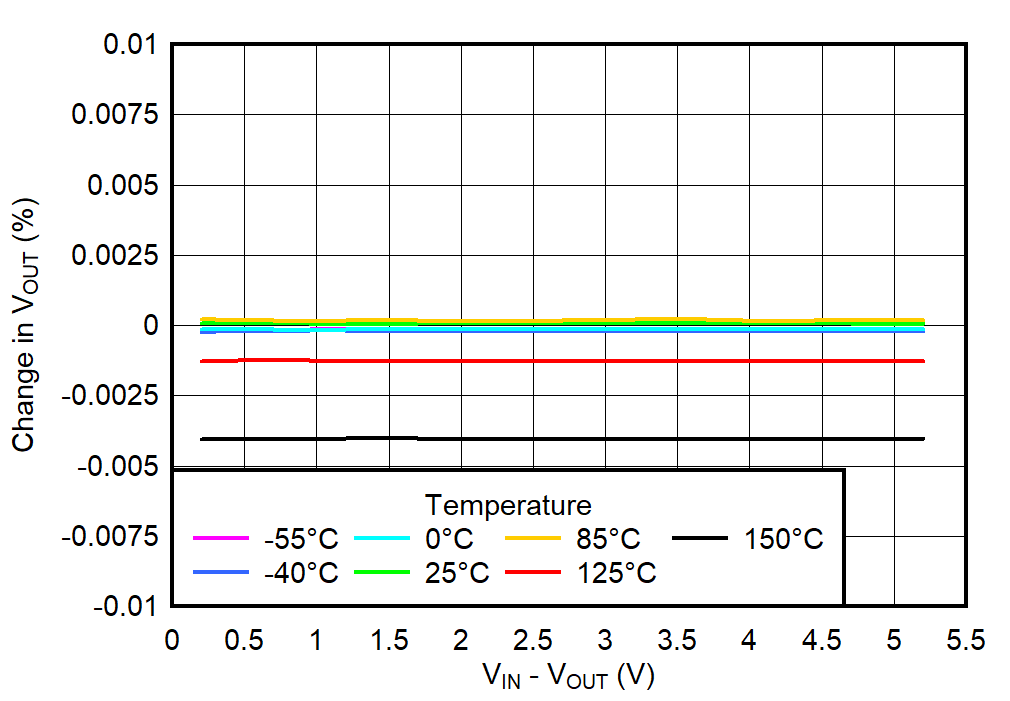 Figure 5-6 Line Regulation
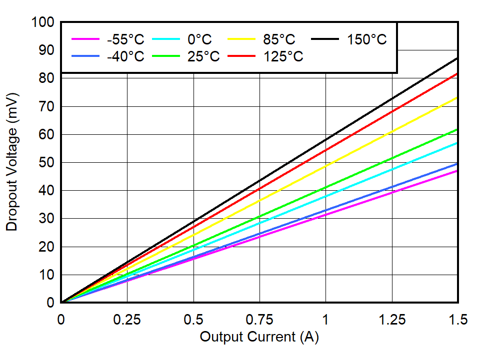 Figure 5-8 VIN Dropout Voltage vs IOUT and Temperature
(TJ)
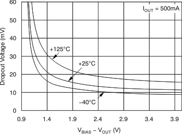 Figure 5-10 VIN Dropout Voltage vs VBIAS – VOUT and Temperature (TJ)
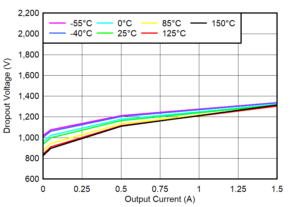 Figure 5-12 VBIAS Dropout Voltage vs IOUT and
Temperature
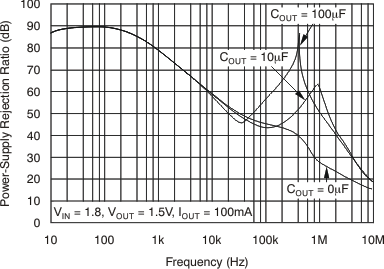 Figure 5-14 VIN PSRR vs Frequency
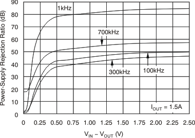 Figure 5-16 VIN PSRR vs VIN – VOUT
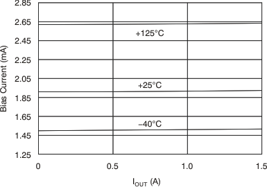 Figure 5-18 IBIAS vs IOUT and Temperature
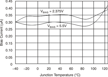 Figure 5-20 IBIAS Shutdown vs Temperature
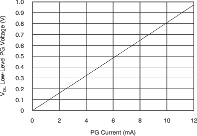 Figure 5-22 Low-Level PG Voltage vs PG Current
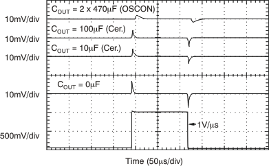 Figure 5-24 VIN Line Transient
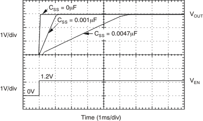 Figure 5-26 Turnon Response
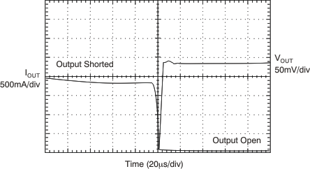 Figure 5-28 Output Short Circuit Recovery