ZHCSHZ5A April   2018  – December 2018 TPS745

PRODUCTION DATA.  

  1. 特性
  2. 应用
  3. 说明
    1.     Device Images
      1.      典型应用
  4. 修订历史记录
  5. Pin Configuration and Functions
    1.     Pin Functions
  6. Specifications
    1. 6.1 Absolute Maximum Ratings
    2. 6.2 ESD Ratings
    3. 6.3 Recommended Operating Conditions
    4. 6.4 Thermal Information
    5. 6.5 Electrical Characteristics
    6. 6.6 Timing Requirements
    7. 6.7 Typical Characteristics
  7. Detailed Description
    1. 7.1 Overview
    2. 7.2 Functional Block Diagram
    3. 7.3 Feature Description
      1. 7.3.1 Undervoltage Lockout (UVLO)
      2. 7.3.2 Shutdown
      3. 7.3.3 Foldback Current Limit
      4. 7.3.4 Thermal Shutdown
    4. 7.4 Device Functional Modes
      1. 7.4.1 Device Functional Mode Comparison
      2. 7.4.2 Normal Operation
      3. 7.4.3 Dropout Operation
      4. 7.4.4 Disabled
  8. Application and Implementation
    1. 8.1 Application Information
      1. 8.1.1 Adjustable Device Feedback Resistors
      2. 8.1.2 Input and Output Capacitor Selection
      3. 8.1.3 Dropout Voltage
      4. 8.1.4 Exiting Dropout
      5. 8.1.5 Reverse Current
      6. 8.1.6 Power Dissipation (PD)
      7. 8.1.7 Power-Good Function
      8. 8.1.8 Feed-Forward Capacitor (CFF)
    2. 8.2 Typical Application
      1. 8.2.1 Design Requirements
      2. 8.2.2 Detailed Design Procedure
        1. 8.2.2.1 Input Current
        2. 8.2.2.2 Thermal Dissipation
      3. 8.2.3 Application Curve
  9. Power Supply Recommendations
  10. 10Layout
    1. 10.1 Layout Guidelines
    2. 10.2 Layout Example
  11. 11器件和文档支持
    1. 11.1 文档支持
      1. 11.1.1 相关文档
    2. 11.2 接收文档更新通知
    3. 11.3 社区资源
    4. 11.4 商标
    5. 11.5 静电放电警告
    6. 11.6 术语表
  12. 12机械、封装和可订购信息

封装选项

机械数据 (封装 | 引脚)
散热焊盘机械数据 (封装 | 引脚)
订购信息

Adjustable Device Feedback Resistors

Figure 44 shows that the output voltage of the TPS745 can be adjusted from 0.55 V to 5.5 V by using a resistor divider network.
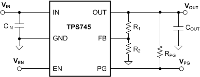
TPS745 simpschem_745_sbvs326.gifFigure 44. Adjustable Operation

The adjustable-version device requires external feedback divider resistors to set the output voltage. VOUT is set using the feedback divider resistors, R1 and R2, according to the following equation:

Equation 2. VOUT = VFB × (1 + R1 / R2)

For this device, VFB = 0.55 V.

To ignore the FB pin current error term in the VOUT equation, set the feedback divider current to 100x the FB pin current listed in the Electrical Characteristics table. This setting provides the maximum feedback divider series resistance, as shown in the following equation:

Equation 3. R1 + R2 ≤ VOUT / (IFB × 100)

For this device, IFB = 10 nA.