ZHCSHM2C June 2018 – May 2022 TPS746-Q1
PRODUCTION DATA
- 1 特性
- 2 应用
- 3 说明
- 4 Revision History
- 5 Pin Configuration and Functions
- 6 Specifications
- 7 Detailed Description
- 8 Application and Implementation
- 9 Power Supply Recommendations
- 10Layout
- 11Device and Documentation Support
封装选项
机械数据 (封装 | 引脚)
散热焊盘机械数据 (封装 | 引脚)
订购信息
8.1.6 Power Dissipation (PD)
Circuit reliability requires consideration of the device power dissipation, location of the circuit on the printed circuit board (PCB), and correct sizing of the thermal plane. The PCB area around the regulator must have few or no other heat-generating devices that cause added thermal stress.
To first-order approximation, power dissipation in the regulator depends on the input-to-output voltage difference and load conditions. Equation 4 calculates power dissipation (PD).
Power dissipation can be minimized, and therefore greater efficiency can be achieved, by correct selection of the system voltage rails. For the lowest power dissipation use the minimum input voltage required for correct output regulation.
For devices with a thermal pad, the primary heat conduction path for the device package is through the thermal pad to the PCB. Solder the thermal pad to a copper pad area under the device. This pad area must contain an array of plated vias that conduct heat to additional copper planes for increased heat dissipation.
The maximum power dissipation determines the maximum allowable ambient temperature (TA) for the device. According to Equation 5, power dissipation and junction temperature are most often related by the junction-to-ambient thermal resistance (RθJA) of the combined PCB and device package and the temperature of the ambient air (TA).
Thermal resistance (RθJA) is highly dependent on the heat-spreading capability built into the particular PCB design, and therefore varies according to the total copper area, copper weight, and location of the planes. The junction-to-ambient thermal resistance listed in the Thermal Information table is determined by the JEDEC standard PCB and copper-spreading area, and is used as a relative measure of package thermal performance.
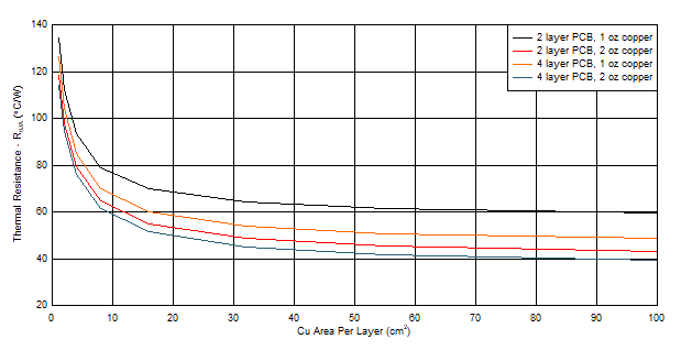
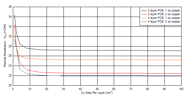
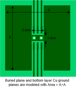
Figure 8-5 and Figure 8-6 show the functions of RθJA and ψJB versus copper area and thickness. These plots are generated with a 101.6-mm × 101.6-mm × 1.6-mm PCB of two and four layers. For the four layer board, the inner planes use 1-oz copper thickness. Outer layers are simulated with both 1-oz and 2-oz copper thickness. A 2 x 1 array of thermal vias of 300-µm drill diameter and 25-µm copper (Cu) plating is located beneath the thermal pad of the device. The thermal vias connect the top layer, the bottom layer and, in the case of the 4-layer board, the first inner GND plane. Each of the layers has a copper plane of equal area, as shown in Figure 8-7.
 Figure 8-5 RθJA versus Cu Area for the WSON (DRV) Package
 Figure 8-6 ψJB versus Cu Area for the WSON (DRV) Package
As shown in Figure 8-7, each of the layers has a copper plane of equal area.
 Figure 8-7 Board Parameters Used for Simulation
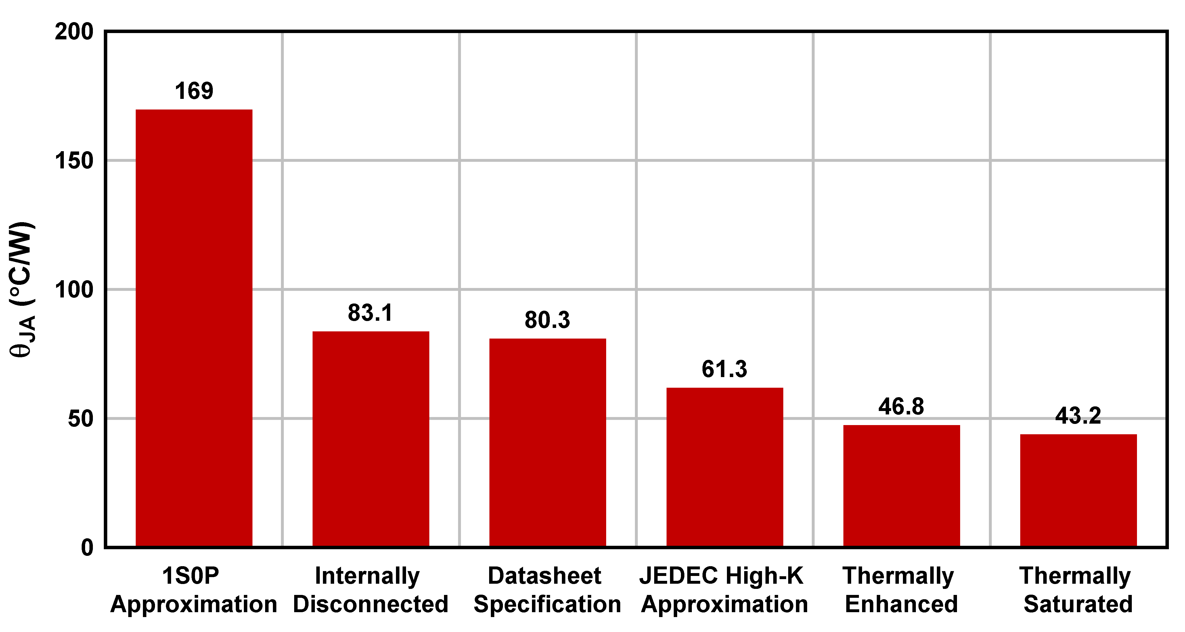
For a more comprehensive study of how thermal resistance varies with copper area and thickness, see the An Empirical Analysis of the Impact of Board Layout on LDO Thermal Performance application report. As shown in Figure 8-8, modifying board layout to be more thermally enhanced can lower the RθJA value from 80.3°C/W to 46.8°C/W or better.
 Figure 8-8 TPS746-Q1 (WSON) RθJA vs Board Layout