ZHCSHZ6A April   2018  – December 2018 TPS746

PRODUCTION DATA.  

  1. 特性
  2. 应用
  3. 说明
    1.     Device Images
      1.      典型应用
  4. 修订历史记录
  5. Pin Configuration and Functions
    1.     Pin Functions
  6. Specifications
    1. 6.1 Absolute Maximum Ratings
    2. 6.2 ESD Ratings
    3. 6.3 Recommended Operating Conditions
    4. 6.4 Thermal Information
    5. 6.5 Electrical Characteristics
    6. 6.6 Timing Requirements
    7. 6.7 Typical Characteristics
  7. Detailed Description
    1. 7.1 Overview
    2. 7.2 Functional Block Diagram
    3. 7.3 Feature Description
      1. 7.3.1 Undervoltage Lockout (UVLO)
      2. 7.3.2 Shutdown
      3. 7.3.3 Foldback Current Limit
      4. 7.3.4 Thermal Shutdown
    4. 7.4 Device Functional Modes
      1. 7.4.1 Device Functional Mode Comparison
      2. 7.4.2 Normal Operation
      3. 7.4.3 Dropout Operation
      4. 7.4.4 Disabled
  8. Application and Implementation
    1. 8.1 Application Information
      1. 8.1.1 Adjustable Device Feedback Resistors
      2. 8.1.2 Input and Output Capacitor Selection
      3. 8.1.3 Dropout Voltage
      4. 8.1.4 Exiting Dropout
      5. 8.1.5 Reverse Current
      6. 8.1.6 Power Dissipation (PD)
      7. 8.1.7 Power-Good Function
    2. 8.2 Feed-Forward Capacitor (CFF)
    3. 8.3 Typical Application
      1. 8.3.1 Design Requirements
      2. 8.3.2 Detailed Design Procedure
        1. 8.3.2.1 Input Current
        2. 8.3.2.2 Thermal Dissipation
      3. 8.3.3 Application Curve
  9. Power Supply Recommendations
  10. 10Layout
    1. 10.1 Layout Guidelines
    2. 10.2 Layout Example
  11. 11器件和文档支持
    1. 11.1 文档支持
      1. 11.1.1 相关文档
    2. 11.2 接收文档更新通知
    3. 11.3 社区资源
    4. 11.4 商标
    5. 11.5 静电放电警告
    6. 11.6 术语表
  12. 12机械、封装和可订购信息

封装选项

机械数据 (封装 | 引脚)
散热焊盘机械数据 (封装 | 引脚)
订购信息

Exiting Dropout

Some applications have transients that place the LDO into dropout, such as slower ramps on VIN during start-up. As with other LDOs, the output may overshoot on recovery from these conditions. A ramping input supply causes an LDO to overshoot on start-up, as shown in Figure 47, when the slew rate and voltage levels are in the correct range. Use an enable signal to avoid this condition.
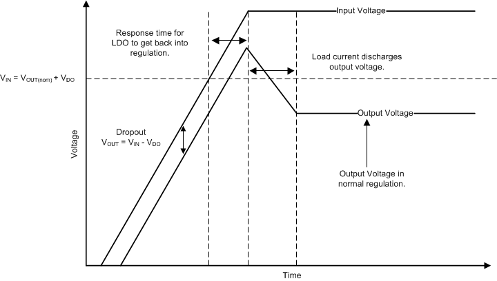
TPS746 ai_startup_into_dropout.gifFigure 47. Startup Into Dropout

Line transients out of dropout can also cause overshoot on the output of the regulator. These overshoots are caused by the error amplifier having to drive the gate capacitance of the pass element and bring the gate back to the correct voltage for proper regulation. Figure 48 illustrates what is happening internally with the gate voltage and how overshoot can be caused during operation. When the LDO is placed in dropout, the gate voltage (VGS) is pulled all the way down to ground to give the pass device the lowest on-resistance as possible. However, if a line transient occurs when the device is in dropout, the loop is not in regulation and can cause the output to overshoot until the loop responds and the output current pulls the output voltage back down into regulation. If these transients are not acceptable, then continue to add input capacitance in the system until the transient is slow enough to reduce the overshoot.
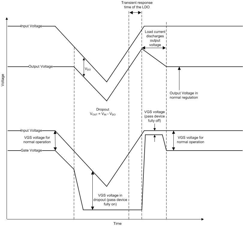
TPS746 LineTransientsFromDropout.gifFigure 48. Line Transients From Dropout