ZHCSN49N January   2007  – June 2024

PRODUCTION DATA  

  1.   1
  2. 特性
  3. 应用
  4. 说明
  5. Pin Configuration and Functions
  6. Specifications
    1. 5.1 Absolute Maximum Ratings
    2. 5.2 ESD Ratings
    3. 5.3 Recommended Operating Conditions
    4. 5.4 Thermal Information
    5. 5.5 Electrical Characteristics
    6. 5.6 Typical Characteristics: IOUT = 50 mA
    7. 5.7 Typical Characteristics: IOUT = 1 A
  7. Detailed Description
    1. 6.1 Overview
    2. 6.2 Functional Block Diagrams
    3. 6.3 Feature Description
      1. 6.3.1 Enable/Shutdown
      2. 6.3.2 Power Good
      3. 6.3.3 Internal Current Limit
      4. 6.3.4 Thermal Protection
    4. 6.4 Device Functional Modes
      1. 6.4.1 Normal Operation
      2. 6.4.2 Dropout Operation
      3. 6.4.3 Disabled
    5. 6.5 Programming
      1. 6.5.1 Programmable Soft-Start
      2. 6.5.2 Sequencing Requirements
  8. Application and Implementation
    1. 7.1 Application Information
      1. 7.1.1 Adjusting the Output Voltage
      2. 7.1.2 Input, Output, and Bias Capacitor Requirements
      3. 7.1.3 Transient Response
      4. 7.1.4 Dropout Voltage
      5. 7.1.5 Output Noise
    2. 7.2 Typical Applications
      1. 7.2.1 FPGA I/O Supply at 1.5 V With a Bias Rail
        1. 7.2.1.1 Design Requirements
        2. 7.2.1.2 Detailed Design Procedure
        3. 7.2.1.3 Application Curves
      2. 7.2.2 FPGA I/O Supply at 1.5 V Without a Bias Rail
        1. 7.2.2.1 Design Requirements
        2. 7.2.2.2 Detailed Design Procedure
        3. 7.2.2.3 Application Curves
    3. 7.3 Power Supply Recommendations
    4. 7.4 Layout
      1. 7.4.1 Layout Guidelines
        1. 7.4.1.1 Estimating Junction Temperature
      2. 7.4.2 Layout Example
  9. Device and Documentation Support
    1. 8.1 Device Support
      1. 8.1.1 Device Nomenclature
      2. 8.1.2 Development Support
        1. 8.1.2.1 Evaluation Modules
        2. 8.1.2.2 Spice Models
    2. 8.2 Documentation Support
      1. 8.2.1 Related Documentation
    3. 8.3 接收文档更新通知
    4. 8.4 支持资源
    5. 8.5 Trademarks
    6. 8.6 静电放电警告
    7. 8.7 术语表
  10. Revision History
  11. 10Mechanical, Packaging, and Orderable Information

封装选项

机械数据 (封装 | 引脚)
散热焊盘机械数据 (封装 | 引脚)
订购信息

Sequencing Requirements

VIN, VBIAS, and VEN can be sequenced in any order without causing damage to the device. However, for the soft-start function to work as intended, certain sequencing rules must be applied. Connecting EN to IN is acceptable for most applications, as long as VIN is greater than 1.1 V and the ramp rate of VIN and VBIAS is faster than the set soft-start ramp rate.

There are several different start-up responses that are possible, but not typical:

  • If the ramp rate of the input sources is slower than the set soft-start time, the output tracks the slower supply minus the dropout voltage until reaching the set output voltage
  • If EN is connected to BIAS, the device soft-starts as programmed, provided that VIN is present before VBIAS
  • If VBIAS and VEN are present before VIN is applied and the set soft-start time has expired, then VOUT tracks VIN
  • If the soft-start time has not expired, the output tracks VIN until VOUT reaches the value set by the charging soft-start capacitor

Figure 6-3 shows the use of an RC-delay circuit to hold off VEN until VBIAS has ramped. This technique can also be used to drive EN from VIN. An external control signal can also be used to enable the device after VIN and VBIAS are present.
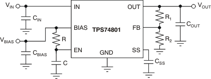
TPS748 Soft-Start Delay Using an RC Circuit to Enable the Device Figure 6-3 Soft-Start Delay Using an RC Circuit to Enable the Device