ZHCSN49N January   2007  – June 2024

PRODUCTION DATA  

  1.   1
  2. 特性
  3. 应用
  4. 说明
  5. Pin Configuration and Functions
  6. Specifications
    1. 5.1 Absolute Maximum Ratings
    2. 5.2 ESD Ratings
    3. 5.3 Recommended Operating Conditions
    4. 5.4 Thermal Information
    5. 5.5 Electrical Characteristics
    6. 5.6 Typical Characteristics: IOUT = 50 mA
    7. 5.7 Typical Characteristics: IOUT = 1 A
  7. Detailed Description
    1. 6.1 Overview
    2. 6.2 Functional Block Diagrams
    3. 6.3 Feature Description
      1. 6.3.1 Enable/Shutdown
      2. 6.3.2 Power Good
      3. 6.3.3 Internal Current Limit
      4. 6.3.4 Thermal Protection
    4. 6.4 Device Functional Modes
      1. 6.4.1 Normal Operation
      2. 6.4.2 Dropout Operation
      3. 6.4.3 Disabled
    5. 6.5 Programming
      1. 6.5.1 Programmable Soft-Start
      2. 6.5.2 Sequencing Requirements
  8. Application and Implementation
    1. 7.1 Application Information
      1. 7.1.1 Adjusting the Output Voltage
      2. 7.1.2 Input, Output, and Bias Capacitor Requirements
      3. 7.1.3 Transient Response
      4. 7.1.4 Dropout Voltage
      5. 7.1.5 Output Noise
    2. 7.2 Typical Applications
      1. 7.2.1 FPGA I/O Supply at 1.5 V With a Bias Rail
        1. 7.2.1.1 Design Requirements
        2. 7.2.1.2 Detailed Design Procedure
        3. 7.2.1.3 Application Curves
      2. 7.2.2 FPGA I/O Supply at 1.5 V Without a Bias Rail
        1. 7.2.2.1 Design Requirements
        2. 7.2.2.2 Detailed Design Procedure
        3. 7.2.2.3 Application Curves
    3. 7.3 Power Supply Recommendations
    4. 7.4 Layout
      1. 7.4.1 Layout Guidelines
        1. 7.4.1.1 Estimating Junction Temperature
      2. 7.4.2 Layout Example
  9. Device and Documentation Support
    1. 8.1 Device Support
      1. 8.1.1 Device Nomenclature
      2. 8.1.2 Development Support
        1. 8.1.2.1 Evaluation Modules
        2. 8.1.2.2 Spice Models
    2. 8.2 Documentation Support
      1. 8.2.1 Related Documentation
    3. 8.3 接收文档更新通知
    4. 8.4 支持资源
    5. 8.5 Trademarks
    6. 8.6 静电放电警告
    7. 8.7 术语表
  10. Revision History
  11. 10Mechanical, Packaging, and Orderable Information

封装选项

机械数据 (封装 | 引脚)
散热焊盘机械数据 (封装 | 引脚)
订购信息

Typical Characteristics: IOUT = 50 mA

at TJ = 25°C, VIN = VOUT(nom) + 0.3 V, VBIAS = 5 V, IOUT = 50 mA, VEN = VIN, CIN = 1 μF, CBIAS = 4.7 μF, and COUT = 10 μF (unless otherwise noted)
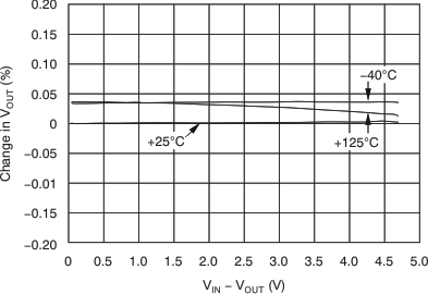
TPS748 VIN Line Regulation
Legacy chip
Figure 5-1 VIN Line Regulation
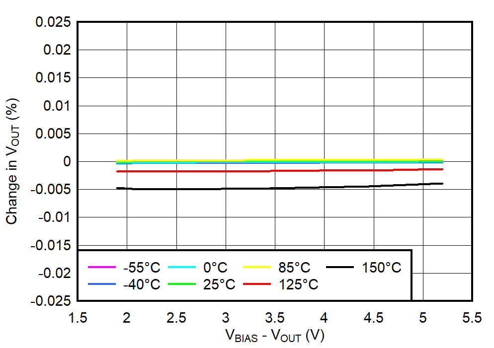
TPS748 VBIAS Line Regulation
Legacy chip
Figure 5-3 VBIAS Line Regulation
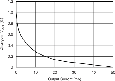
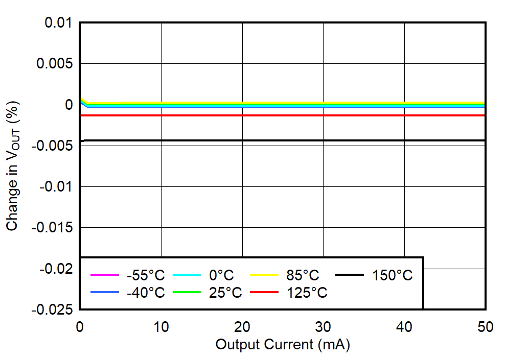
TPS748 Load
                        Regulation at Light Load
 
Figure 5-5 Load Regulation at Light Load
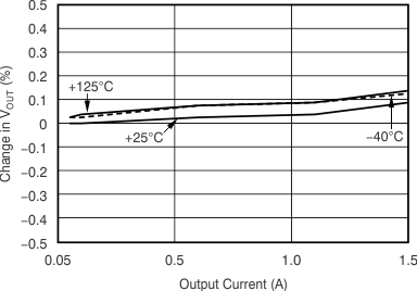
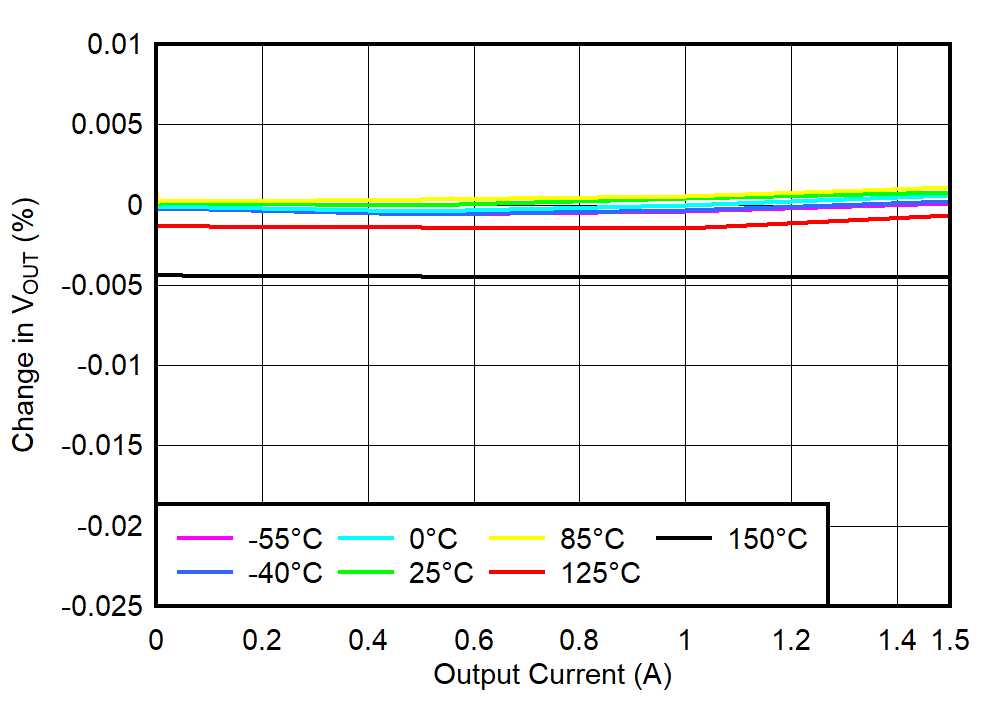
TPS748 Load Regulation
Legacy chip
Figure 5-7 Load Regulation
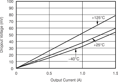
TPS748 VIN Dropout Voltage vs IOUT and Temperature
                            (TJ)
Legacy chip
Figure 5-9 VIN Dropout Voltage vs IOUT and Temperature (TJ)
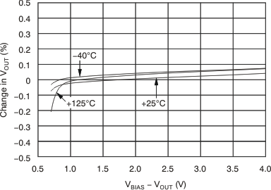
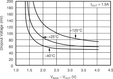
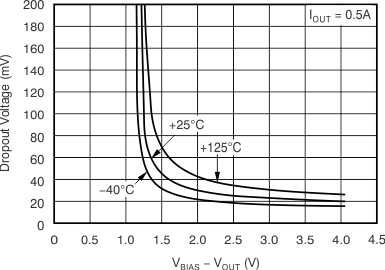
TPS748 VIN Dropout Voltage vs (VBIAS – VOUT)
                        and Temperature (TJ)
 
Figure 5-11 VIN Dropout Voltage vs (VBIAS – VOUT) and Temperature (TJ)
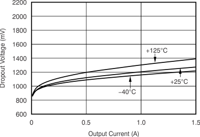
TPS748 VBIAS Dropout Voltage vs IOUT and Temperature
                            (TJ)
Legacy chip
Figure 5-13 VBIAS Dropout Voltage vs IOUT and Temperature (TJ)
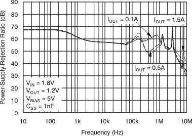
TPS748 VBIAS PSRR vs Frequency
Legacy chip
Figure 5-15 VBIAS PSRR vs Frequency
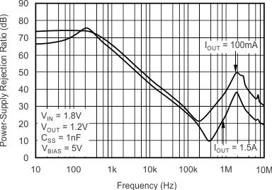
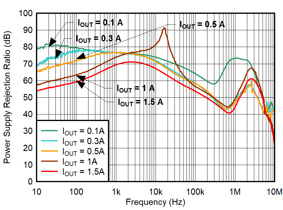
TPS748 VIN PSRR vs Frequency
Legacy chip
Figure 5-17 VIN PSRR vs Frequency
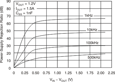
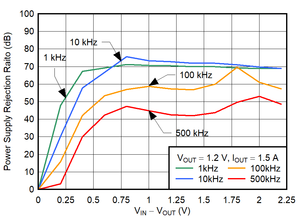
TPS748 VIN PSRR vs (VIN – VOUT)
Legacy chip
Figure 5-19 VIN PSRR vs (VIN – VOUT)
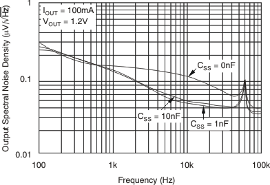
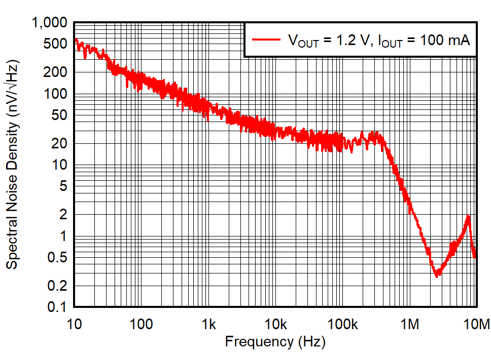
TPS748 Noise
                        Spectral Density
Legacy chip
Figure 5-21 Noise Spectral Density
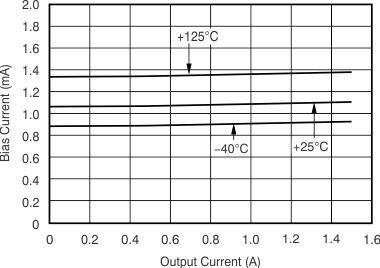
TPS748 BIAS
                        Pin Current vs Output Current and Temperature (TJ)
Legacy chip
Figure 5-23 BIAS Pin Current vs Output Current and Temperature (TJ)
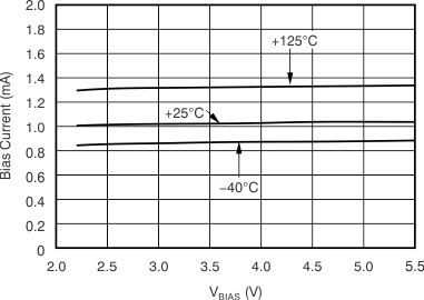
TPS748 BIAS
                        Pin Current vs VBIAS and Temperature (TJ)
Legacy chip
Figure 5-25 BIAS Pin Current vs VBIAS and Temperature (TJ)
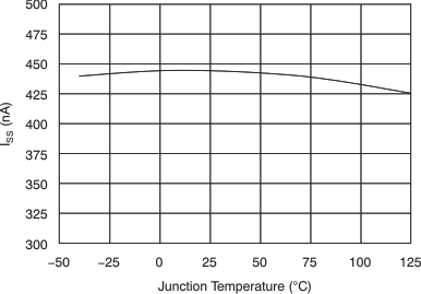
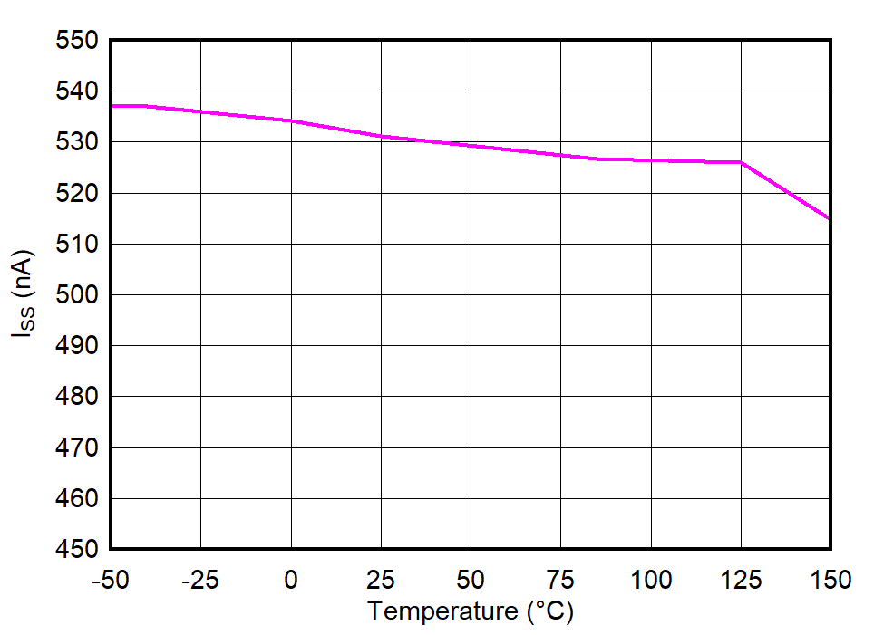
TPS748 Soft-Start Charging Current (ISS) vs Temperature
                        (TJ)
Legacy chip
Figure 5-27 Soft-Start Charging Current (ISS) vs Temperature (TJ)
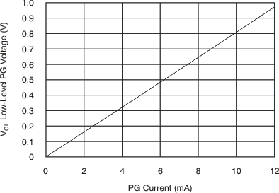
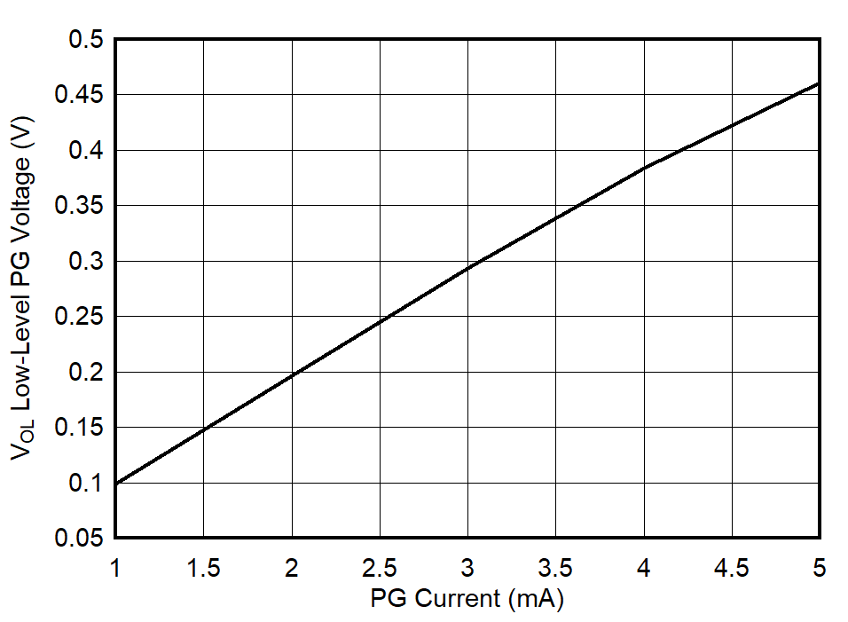
TPS748 Low-Level PG Voltage vs Current
Legacy chip
Figure 5-29 Low-Level PG Voltage vs Current
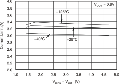
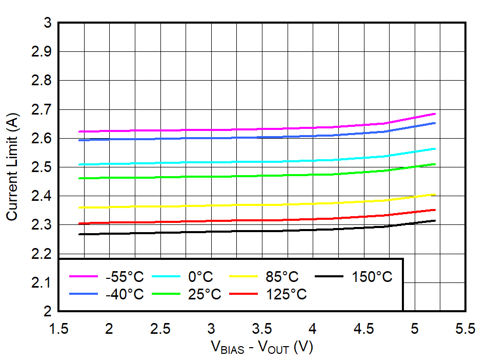
TPS748 Current Limit vs (VBIAS – VOUT)
Legacy chip
Figure 5-31 Current Limit vs (VBIAS – VOUT)
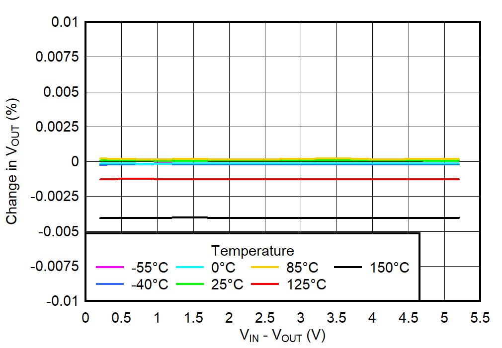
TPS748 VIN Line Regulation
New chip
Figure 5-2 VIN Line Regulation
TPS748 VBIAS Line Regulation
New chip
Figure 5-4 VBIAS Line Regulation
TPS748 Load
                        Regulation at Light Load
New chip
Figure 5-6 Load Regulation at Light Load
TPS748 Load Regulation
New chip
Figure 5-8 Load Regulation
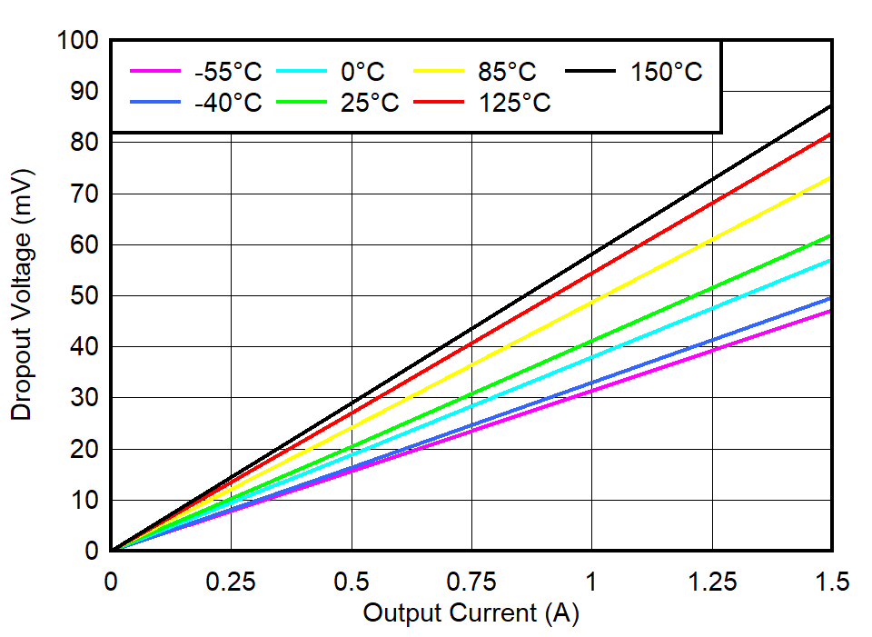
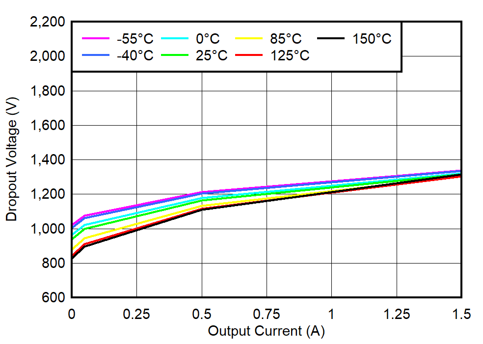
TPS748 VIN Dropout Voltage vs IOUT
                        and Temperature (TJ)
New chip
Figure 5-10 VIN Dropout Voltage vs IOUT and Temperature (TJ)
TPS748 VIN Dropout Voltage vs (VBIAS – VOUT)
                        and Temperature (TJ)
 
Figure 5-12 VIN Dropout Voltage vs (VBIAS – VOUT) and Temperature (TJ)
TPS748 VBIAS Dropout Voltage vs IOUT
                        and Temperature (TJ)
New chip
Figure 5-14 VBIAS Dropout Voltage vs IOUT and Temperature (TJ)
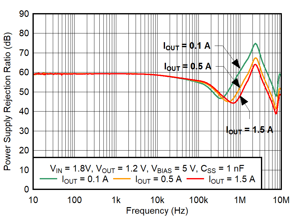
TPS748 VBIAS PSRR vs Frequency
New chip
Figure 5-16 VBIAS PSRR vs Frequency
TPS748 VIN PSRR vs Frequency
 
Figure 5-18 VIN PSRR vs Frequency
TPS748 VIN PSRR vs (VIN –
                            VOUT)
New chip
Figure 5-20 VIN PSRR vs (VIN – VOUT)
TPS748 Noise Spectral Density
New chip
Figure 5-22 Noise Spectral Density
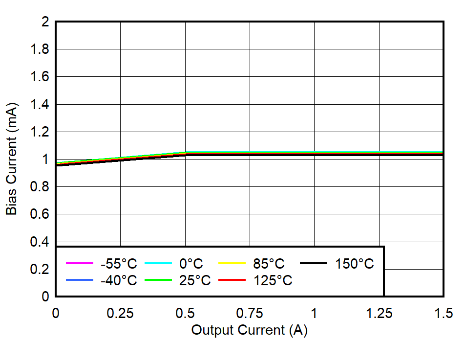
TPS748 BIAS Pin Current vs Output Current and Temperature
                            (TJ)
New chip
Figure 5-24 BIAS Pin Current vs Output Current and Temperature (TJ)
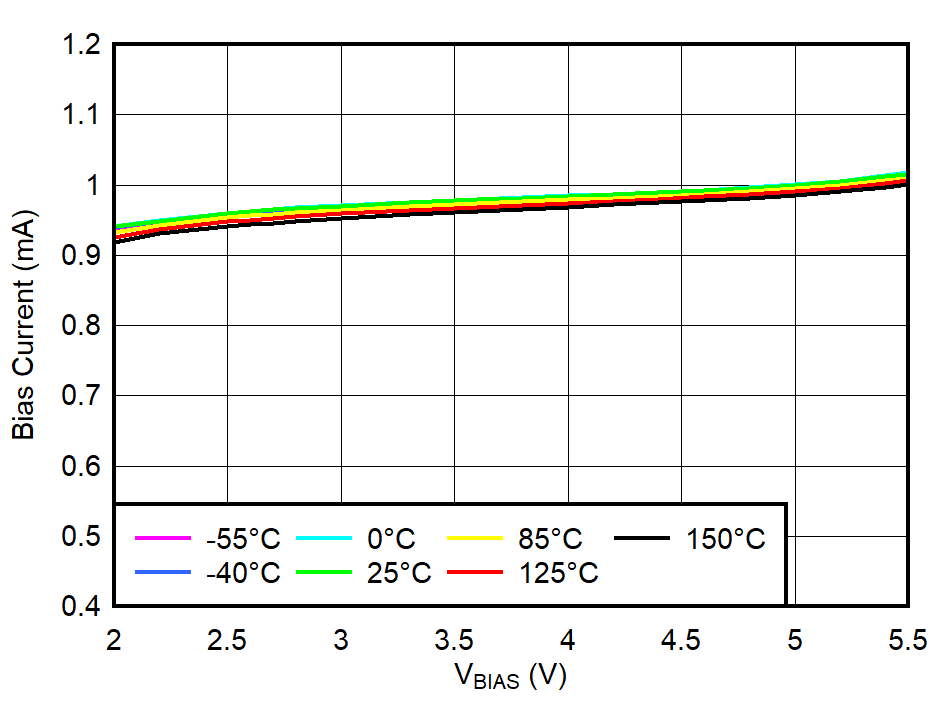
TPS748 BIAS Pin Current vs VBIAS and Temperature
                            (TJ)
New chip
Figure 5-26 BIAS Pin Current vs VBIAS and Temperature (TJ)
TPS748 Soft-Start Charging Current (ISS) vs
                        Temperature (TJ)
New chip
Figure 5-28 Soft-Start Charging Current (ISS) vs Temperature (TJ)
TPS748 Low-Level PG Voltage vs Current
New chip
Figure 5-30 Low-Level PG Voltage vs Current
TPS748 Current Limit vs (VBIAS –
                        VOUT)
New chip
Figure 5-32 Current Limit vs (VBIAS – VOUT)