SBVS080J September 2006 – November 2016 TPS75100 , TPS75103 , TPS75105
PRODUCTION DATA.
- 1 Features
- 2 Applications
- 3 Description
- 4 Revision History
- 5 Pin Configuration and Functions
- 6 Specifications
- 7 Detailed Description
- 8 Application and Implementation
- 9 Power Supply Recommendations
- 10Layout
- 11Device and Documentation Support
- 12Mechanical, Packaging, and Orderable Information
封装选项
请参考 PDF 数据表获取器件具体的封装图。
机械数据 (封装 | 引脚)
- DSK|10
- YFF|9
散热焊盘机械数据 (封装 | 引脚)
- DSK|10
订购信息
6 Specifications
6.1 Absolute Maximum Ratings
over operating free-air temperature range (unless otherwise noted)| MIN | MAX | UNIT | |
|---|---|---|---|
| VIN range | –0.3 | 7 | V |
| VISET, VENA, VENB, VDX range | –0.3 | VIN | V |
| IDX for D1A, D2A, D1B, D2B | 35 | mA | |
| D1A, D2A, D1B, D2B short-circuit duration | Indefinite | ||
| Continuous total power dissipation | Internally limited | ||
| Junction temperature, TJ | –55 | 150 | °C |
| Storage temperature, Tstg | –55 | 150 | °C |
6.2 ESD Ratings
| VALUE | UNIT | |||
|---|---|---|---|---|
| V(ESD) | Electrostatic discharge | Human-body model (HBM), per ANSI/ESDA/JEDEC JS-001(1) | ±2000 | V |
| Charged-device model (CDM), per JEDEC specification JESD22-C101(2) | ±500 | |||
(1) JEDEC document JEP155 states that 500-V HBM allows safe manufacturing with a standard ESD control process.
(2) JEDEC document JEP157 states that 250-V CDM allows safe manufacturing with a standard ESD control process.
6.3 Recommended Operating Conditions
| PARAMETER | MIN | NOM | MAX | UNIT | |
|---|---|---|---|---|---|
| VIN | Input voltage | 2.7 | 5.5 | V | |
| IDX | Operating current per LED | 3 | 25 | mA | |
| tPWM | On-time for PWM signal | 33 | µs | ||
| TJ | Operating junction temperature range | –40 | 85 | °C | |
6.4 Thermal Information
| THERMAL METRIC(1) | TPS7510x | UNIT | ||
|---|---|---|---|---|
| YFF (DSBGA) | DSK (WSON) | |||
| 9 PINS | 10 PINS | |||
| RθJA | Junction-to-ambient thermal resistance | 101.6 | 65.3 | °C/W |
| RθJC(top) | Junction-to-case (top) thermal resistance | 1.2 | 54.0 | °C/W |
| RθJB | Junction-to-board thermal resistance | 17.6 | 39.5 | °C/W |
| ψJT | Junction-to-top characterization parameter | 0.6 | 1.6 | °C/W |
| ψJB | Junction-to-board characterization parameter | 17.8 | 39.7 | °C/W |
| RθJC(bot) | Junction-to-case (bottom) thermal resistance | N/A | 23.6 | °C/W |
(1) For more information about traditional and new thermal metrics, see the Semiconductor and IC Package Thermal Metrics application report.
6.5 Electrical Characteristics
over operating junction temperature range (TJ = –40°C to +85°C), VIN = 3.8 V, DxA and DxB = 3.3 V, RSET = 32.4 kΩ, and ENA and ENB = 3.8 V (unless otherwise noted); typical values are at TA = 25°C| PARAMETER | TEST CONDITIONS | MIN | TYP | MAX | UNIT | |||
|---|---|---|---|---|---|---|---|---|
| ISHDN | Shutdown supply current | VENA,B = 0 V, VDX = 0 V | 0.03 | 1 | µA | |||
| IGND | Ground current | DSK package | IDX ≤ 5 mA, VIN = 3.8 V | 170 | 230 | µA | ||
| IDX > 5 mA, VIN = 3.8 V | 250 | 300 | ||||||
| YFF package | IDX ≤ 5 mA, VIN = 4.5 V | 170 | 200 | |||||
| IDX > 5 mA, VIN = 4.5 V | 250 | 300 | ||||||
| ΔID | Current matching (IDXMAX – IDXMIN / IDXMAX) × 100% |
TA = 25°C | 0% | 2% | 4% | |||
| TA = –40°C to +85°C | YFF package | 0% | 5% | |||||
| DSK package | 0% | 6% | ||||||
| ΔIDX%/ΔVIN | Line regulation | 3.5 V ≤ VIN ≤ 4.5 V, IDX = 5 mA | 2.0 | %/V | ||||
| ΔIDX%/ΔVDX | Load regulation | 1.8 V ≤ VDX ≤ 3.5 V, IDX = 5 mA | 0.8 | %/V | ||||
| VDO | Dropout voltage of any DX current source (VDX at IDX = 0.8 × IDX, nom) |
IDXnom = 5 mA | 28 | 100 | mV | |||
| IDXnom = 15 mA | 70 | |||||||
| VISET | Reference voltage for current set | 1.183 | 1.225 | 1.257 | V | |||
| IOPEN | Diode current accuracy(1) | ISET = open, VDX = VIN – 0.2 V |
YFF package | 0.5% | 3% | |||
| DSK package | 0.5% | 4% | ||||||
| ISET | ISET pin current range | 2.5 | 62.5 | µA | ||||
| k | ISET to IDX current ratio(1) | 420 | ||||||
| VIH | Enable high level input voltage | 1.2 | V | |||||
| VIL | Enable low level input voltage | 0.4 | V | |||||
| IINA | Enable pin A (VENA) input current | VENA = 3.8 V | 5.0 | 6.1 | µA | |||
| VENA = 1.8 V | 2.2 | |||||||
| IINB | Enable pin B (VENB) input current | VENB = 3.8 V | 4.0 | 4.9 | µA | |||
| VENB = 1.8 V | 1.8 | |||||||
| tSD | Shutdown delay time | Delay from ENA and ENB = low to reach shutdown current (IDX = 0.1 × IDX, nom) |
5 | 13 | 30 | µs | ||
| TSD | Thermal shutdown temperature | Shutdown, temperature increasing | 165 | °C | ||||
| Reset, temperature decreasing | 140 | |||||||
(1) Average of all four IDX outputs.
6.6 Typical Characteristics
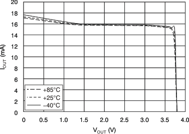
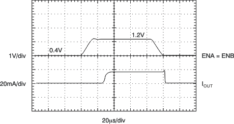
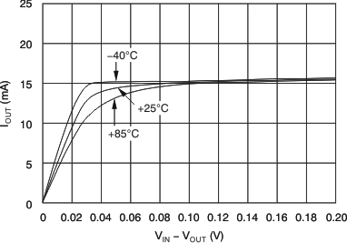
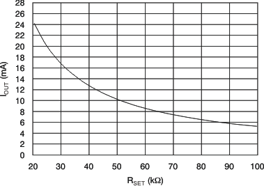
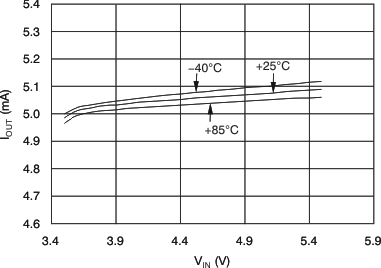
over operating junction temperature range (TJ = –40°C to +85°C), VIN = 3.8 V, DxA and DxB = 3.3 V, RSET = 32.4 kΩ, and ENA and ENB = high (unless otherwise noted); typical values are at TA = 25°C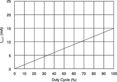
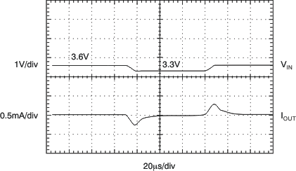
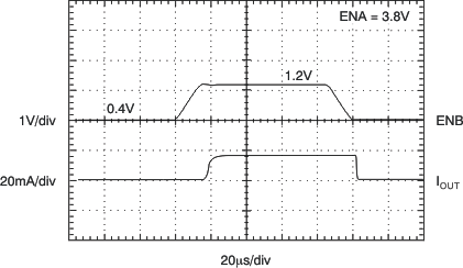
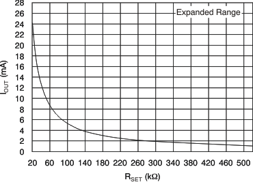
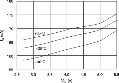
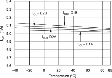
RSET = Open
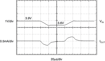
RSET = Open
