SBVS080J September 2006 – November 2016 TPS75100 , TPS75103 , TPS75105
PRODUCTION DATA.
- 1 Features
- 2 Applications
- 3 Description
- 4 Revision History
- 5 Pin Configuration and Functions
- 6 Specifications
- 7 Detailed Description
- 8 Application and Implementation
- 9 Power Supply Recommendations
- 10Layout
- 11Device and Documentation Support
- 12Mechanical, Packaging, and Orderable Information
封装选项
请参考 PDF 数据表获取器件具体的封装图。
机械数据 (封装 | 引脚)
- DSK|10
- YFF|9
散热焊盘机械数据 (封装 | 引脚)
- DSK|10
订购信息
5 Pin Configuration and Functions
YFF Package
9-Pin DSBGA
Top View

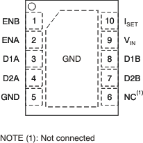
DSK Package
10-Pin WSON
Top View

Pin Functions
| PIN | I/O | DESCRIPTION | ||
|---|---|---|---|---|
| NAME | WCSP | WSON | ||
| ENA | A3 | 2 | I | Enable pin, Bank A. Driving this pin high turns on the current source to Bank A outputs. Driving this pin low turns off the current source to Bank A outputs. An applied PWM signal reduces the LED current (between 0 mA and the maximum current set by ISET) as a function of the duty cycle of the PWM signal. ENA and ENB can be tied together. ENA can be left OPEN or connected to GND if not used. See the Application and Implementation section for more details. |
| D1A | B3 | 3 | O | Diode source current output, Bank A. Connect to LED anode. |
| D2A | C3 | 4 | O | Diode source current output, Bank A. Connect to LED anode. |
| ENB | A2 | 1 | I | Enable pin, Bank B. Driving this pin high turns on the current source to Bank B outputs. Driving this pin low turns off the current source to Bank B outputs. An applied PWM signal reduces the LED current (between 0 mA and the maximum current set by ISET) as a function of the duty cycle of the PWM signal. ENA and ENB can be tied together. ENB can be left OPEN or connected to GND if not used. See the Application and Implementation section for more details. |
| VIN | B2 | 9 | I | Supply input |
| GND | C2 | 5, Pad | — | Ground |
| ISET | A1 | 10 | I | An optional resistor can be connected between this pin and GND to set the maximum current through the LEDs. If no resistor is connected, ISET defaults to the internally programmed value. |
| D1B | B1 | 8 | O | Diode source current output, Bank B. Connect to LED anode. |
| D2B | C1 | 7 | O | Diode source current output, Bank B. Connect to LED anode. |
| NC | — | 6 | — | Not internally connected |