ZHCSKA6J December 1998 – September 2019 TPS763
PRODUCTION DATA.
6.6 Typical Characteristics
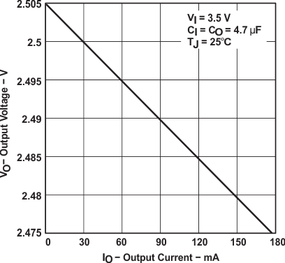 Figure 1. TPS76325 Output Voltage
vs Output Current
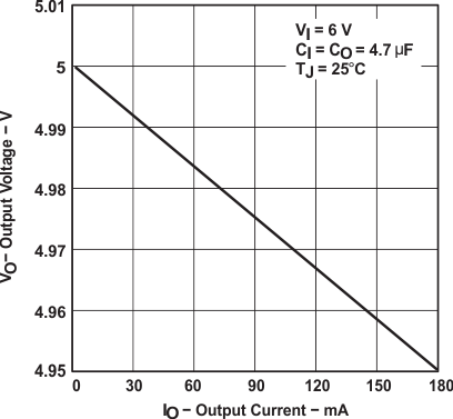 Figure 3. TPS76350 Output Voltage
vs Output Current
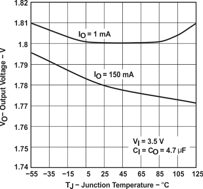 Figure 5. TPS76318 Output Voltage
vs Free-Air Temperature
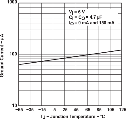 Figure 7. TPS76350 Ground Current
vs Free-Air Temperature
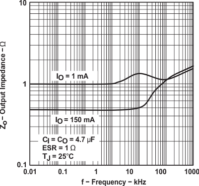 Figure 9. Output Impedance vs Frequency
 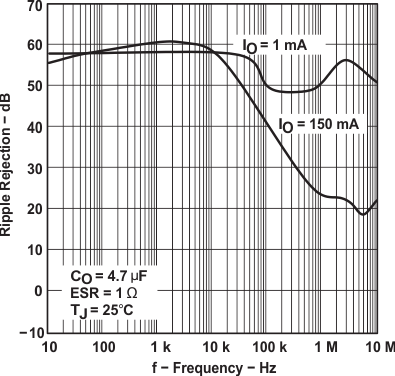 Figure 11. TPS76325 Ripple Rejection vs Frequency
 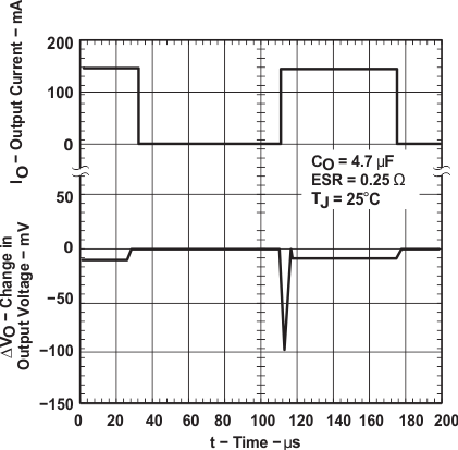 Figure 13. TPS76318 Load Transient Response
 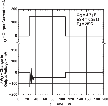 Figure 15. TPS76350 Load Transient Response
 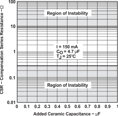 Figure 17. Compensation Series Resistance (CSR)
vs Added Ceramic Capacitance
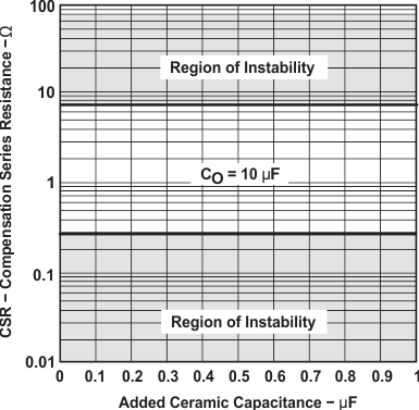 Figure 19. Compensation Series Resistance (CSR) vs Added Ceramic Capacitance
 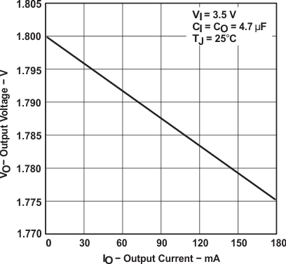 Figure 2. TPS76318 Output Voltage
vs Output Current
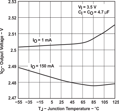 Figure 4. TPS76325 Output Voltage
vs Output Current
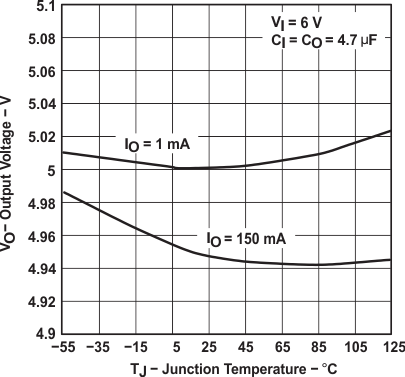 Figure 6. TPS76350 Output Voltage
vs Free-Air Temperature
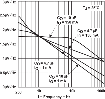 Figure 8. Output Noise vs Frequency
 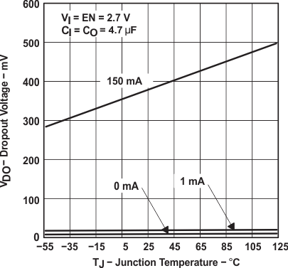 Figure 10. TPS76325 Dropout Voltage
vs Free-Air Temperature
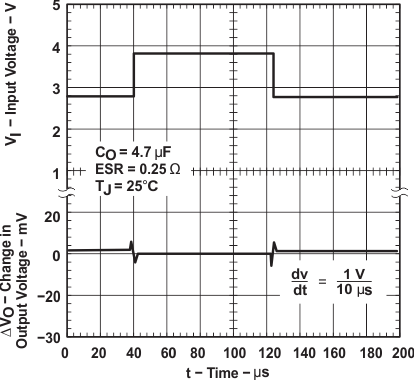 Figure 12. TPS76318 Line Transient Response
 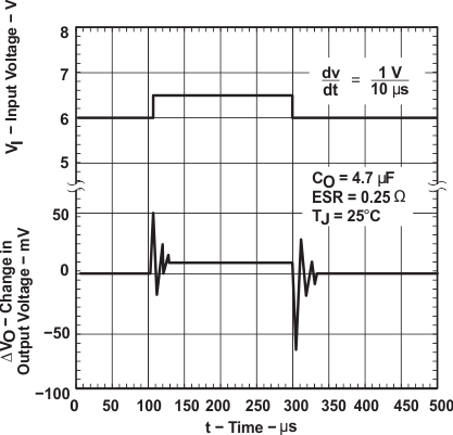 Figure 14. TPS76350 Line Transient Response
 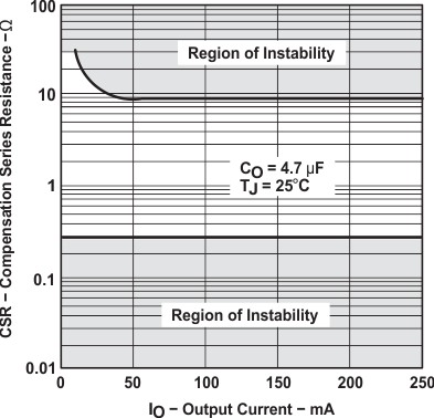 Figure 16. Compensation Series Resistance (CSR)
vs Output Current
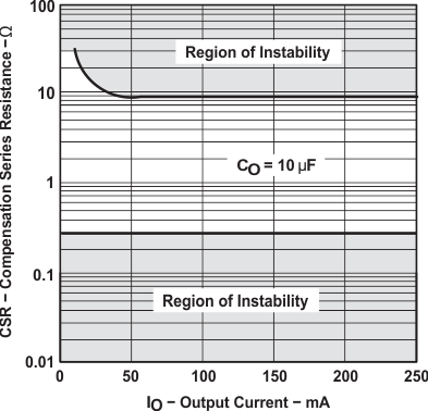 Figure 18. Compensation Series Resistance (CSR)
vs Output Current