7 Specifications
7.1 Absolute Maximum Ratings
over operating free-air temperature range (unless otherwise noted) (1)
|
MIN |
MAX |
UNIT |
| VI |
Input voltage range(2) |
–0.3 |
13.5 |
V |
|
Voltage range at EN |
–0.3 |
VI + 0.3 |
V |
|
Maximum RESET voltage |
|
16.5 |
|
|
Peak output current |
Internally limited |
|
| VO |
Output voltage (OUT, FB) |
|
7 |
V |
|
Continuous total power dissipation |
See Thermal Information |
|
| TJ |
Operating junction temperature range |
–40 |
125 |
°C |
| Tstg |
Storage temperature range |
−65 |
150 |
°C |
(1) Stresses beyond those listed under Absolute Maximum Ratings may cause permanent damage to the device. These are stress ratings only, which do not imply functional operation of the device at these or any other conditions beyond those indicated under Recommended Operating Conditions. Exposure to absolute-maximum-rated conditions for extended periods may affect device reliability.
(2) All voltage values are with respect to network terminal ground.
7.2 ESD Ratings
|
VALUE |
UNIT |
| V(ESD) |
Electrostatic discharge |
Human body model (HBM), per ANSI/ESDA/JEDEC JS-001, all pins(1) |
2000 |
V |
(1) JEDEC document JEP155 states that 500-V HBM allows safe manufacturing with a standard ESD control process.
7.3 Recommended Operating Conditions
over operating free-air temperature range (unless otherwise noted)
|
|
MIN |
MAX |
UNIT |
| VI(1) |
Input voltage |
2.7 |
10 |
V |
| VO |
Output voltage range |
1.2 |
5.5 |
V |
| IO(2) |
Output current |
0 |
1.0 |
A |
| TJ(2) |
Operating junction temperature |
–40 |
125 |
°C |
(1) Maximum VIN = VOUT + VDO or 2.7V, whichever is greater.
(2) Continuous current and operating junction temperature are limited by internal protection circuitry, but it is not recommended that the device operate under conditions beyond those specified in this table for extended periods of time.
7.4 Thermal Information
| THERMAL METRIC(1) |
TPS767xxQ |
UNIT |
| PWP (HTSSOP) |
D (SOIC) |
| (20 PINS) |
(8 PINS) |
| RθJA |
Junction-to-ambient thermal resistance |
35.8 |
106.9 |
°C/W |
| RθJC(top) |
Junction-to-case (top) thermal resistance |
26.1 |
52.5 |
°C/W |
| RθJB |
Junction-to-board thermal resistance |
8.7 |
47.7 |
°C/W |
| ψJT |
Junction-to-top characterization parameter |
0.4 |
9.0 |
°C/W |
| ψJB |
Junction-to-board characterization parameter |
8.6 |
47.1 |
°C/W |
| RθJC(bot) |
Junction-to-case (bottom) thermal resistance |
2.6 |
n/a |
°C/W |
(1) For more information about traditional and new thermal metrics, see the
Semiconductor and IC Package Thermal Metrics application report,
SPRA953.
7.5 Electrical Characteristics
VI = VO(typ) + 1 V, IO = 1 mA, EN = 0 V, Co = 10 µF (over recommended operating free-air temperature range, unless otherwise noted)
| PARAMETER |
TEST CONDITIONS |
MIN |
TYP |
MAX |
UNIT |
Output voltage
(10 µA to 1 A load) |
TPS76701 |
1.5 V ≤ VO ≤ 5.5 V, |
TJ = 25°C |
|
VO |
|
V |
| 1.5 V ≤ VO ≤ 5.5 V, |
TJ = −40°C to 125°C |
0.98VO |
|
1.02VO |
| TPS76715 |
TJ = 25°C, |
2.7 V < VIN < 10 V |
|
1.5 |
|
V |
| TJ = −40°C to 125°C, |
2.7 V < VIN < 10 V |
1.470 |
|
1.530 |
| TPS76718 |
TJ = 25°C, |
2.8 V < VIN < 10 V |
|
1.8 |
|
V |
| TJ = −40°C to 125°C, |
2.8 V < VIN < 10 V |
1.7646 |
|
1.836 |
| TPS76725 |
TJ = 25°C, |
3.5 V < VIN < 10 V |
|
2.5 |
|
V |
| TJ = −40°C to 125°C, |
3.5 V < VIN < 10 V |
2.450 |
|
2.550 |
| TPS76727 |
TJ = 25°C, |
3.7 V < VIN < 10 V |
|
2.7 |
|
V |
| TJ = −40°C to 125°C, |
3.7 V < VIN < 10 V |
2.646 |
|
2.754 |
| TPS76728 |
TJ = 25°C, |
3.8 V < VIN < 10 V |
|
2.8 |
|
V |
| TJ = −40°C to 125°C, |
3.8 V < VIN < 10 V |
2.7446 |
|
2.856 |
| TPS76730 |
TJ = 25°C, |
4.0 V < VIN < 10 V |
|
3 |
|
V |
| TJ = −40°C to 125°C, |
4.0 V < VIN < 10 V |
2.9400 |
|
3.060 |
| TPS76733 |
TJ = 25°C, |
4.3 V < VIN < 10 V |
|
3.3 |
|
|
| TJ = −40°C to 125°C, |
4.3 V < VIN < 10 V |
3.2346 |
|
3.366 |
|
| TPS76750 |
TJ = 25°C, |
6.0 V < VIN < 10 V |
|
5 |
|
|
| TJ = −40°C to 125°C, |
6.0 V < VIN < 10 V |
4.900 |
|
5.100 |
|
| Quiescent current (GND current) EN = 0V |
10 µA < IO < 1 A, |
TJ = 25°C |
|
85 |
|
µA |
| IO = 1 A, |
TJ = −40°C to 125°C |
|
|
125 |
| Output voltage line regulation (∆VO/VO) |
VO + 1 V < VI ≤ 10 V, |
TJ = 25°C |
|
0.01 |
|
%/V |
| Load regulation |
|
|
|
3 |
|
mV |
| Output noise voltage |
TPS76718 |
BW = 200 Hz to 100 kHz,
Co = 10 µF, |
IC = 1 A,
TJ = 25°C |
|
55 |
|
µVrms |
| Output current limit |
VO = 0 V |
|
1.2 |
1.7 |
2 |
A |
| Thermal shutdown junction temperature |
|
|
|
150 |
|
°C |
| Standby current |
EN = VI, |
TJ = 25°C, 2.7 V < VI < 10 V |
|
1 |
|
µA |
EN = VI,
|
TJ = −40°C to 125°C,
2.7 V < VI < 10 V |
|
|
10 |
µA |
| FB input current |
TPS76701 |
FB = 1.5 V |
|
|
2 |
|
nA |
| High level enable input voltage |
|
|
1.7 |
|
|
V |
| Low level enable input voltage |
|
|
|
|
0.9 |
V |
| Power supply ripple rejection |
f = 1 kHz, Co = 10 µF, |
TJ = 25°C |
|
60 |
|
dB |
| Reset |
Minimum input voltage for valid RESET |
IO(RESET) = 300 μA |
|
|
1.1 |
|
|
| Trip threshold voltage |
VO decreasing |
|
92 |
|
98 |
|
| Hysteresis voltage |
Measured at VO |
|
|
0.5 |
|
|
| Output low voltage |
VI = 2.7 V, |
IO(RESET) = 1 mA |
|
0.15 |
0.4 |
|
| Leakage current |
V(RESET) = 5 V |
|
|
|
1 |
|
| RESET time-out delay |
|
|
|
200 |
|
|
| Input current (EN) |
EN = 0 V |
|
–1 |
0 |
1 |
µA |
| EN = VI |
|
–1 |
|
1 |
| Dropout voltage (1) |
TPS76728 |
IO = 1 A |
TJ = 25°C |
|
500 |
|
mV |
| TJ = −40°C to 125°C |
|
|
825 |
| TPS76730 |
IO = 1 A |
TJ = 25°C |
|
450 |
|
mV |
| TJ = −40°C to 125°C |
|
|
675 |
| TPS76733 |
IO = 1 A |
TJ = 25°C |
|
350 |
|
mV |
| TJ = −40°C to 125°C |
|
|
575 |
| TPS76750 |
IO = 1 A |
TJ = 25°C |
|
230 |
|
mV |
| TJ = −40°C to 125°C |
|
|
380 |
(1) IN voltage equals VO(typ) − 100 mV; TPS76701 output voltage set to 3.3 V nominal with external resistor divider. TPS76715, TPS76718, TPS76725, and TPS76727 dropout voltage limited by input voltage range limitations (i.e., TPS76730 input voltage needs to drop to 2.9 V for purpose of this test).
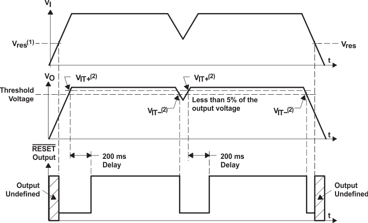 Figure 1. Timing Diagram
 Figure 1. Timing Diagram
