SGLS155B February 2003 – November 2016 TPS768-Q1
PRODUCTION DATA.
- 1 Features
- 2 Applications
- 3 Description
- 4 Revision History
- 5 Pin Configuration and Functions
- 6 Specifications
- 7 Parameter Measurement Information
- 8 Detailed Description
- 9 Application and Implementation
- 10Power Supply Recommendations
- 11Layout
- 12Device and Documentation Support
- 13Mechanical, Packaging, and Orderable Information
9 Application and Implementation
NOTE
Information in the following applications sections is not part of the TI component specification, and TI does not warrant its accuracy or completeness. TI’s customers are responsible for determining suitability of components for their purposes. Customers should validate and test their design implementation to confirm system functionality.
9.1 Application Information
The TPS768xx-Q1 device is offered in 1.8-V, 2.5-V, 3.3-V, and 5-V fixed-voltage versions and in an adjustable version (programmable over the range of 1.2 V to 5.5 V). Output voltage tolerance is specified as a maximum of ±2% over line, load, and temperature ranges.
9.2 Typical Application
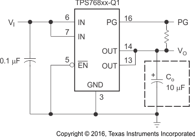
 Figure 22. Typical Application Configuration (for Fixed-Output Options)
9.2.1 Design Requirements
For this design example use, the parameters listed in the following table as the input parameters.
| PARAMETER | EXAMPLE VALUE |
|---|---|
| Input voltage range | 2.7 V to 10 V |
| Output voltage | Fixed: 1.8 V, 2.5 V, 3. 3 V, and 5 V Adjustable: 1.2 V to 5.5 V |
| Output current rating | 1 A |
| Output capacitor range | >10 µF |
| Output capacitor ESR range | 50 mΩ to 1.5 Ω |
9.2.2 Detailed Design Procedure
9.2.2.1 Minimum Load Requirements
The TPS768xx-Q1 family is stable even at zero load; no minimum load is required for operation.
9.2.2.2 FB Pin Connection (Adjustable Version Only)
The FB pin is an input pin to sense the output voltage and close the loop for the adjustable version. The output voltage is sensed through a resistor-divider network to close the loop as shown in Figure 23. Normally, this connection should be as short as possible; however, the connection can be made near a critical circuit to improve performance at that point. Internally, FB connects to a high-impedance wide-bandwidth amplifier, and noise pickup feeds through to the regulator output. Routing the FB connection to minimize or avoid noise pickup is essential.
9.2.2.3 Programming the TPS76801-Q1 Adjustable LDO Regulator
The output voltage of the TPS76801-Q1 adjustable regulator is programmed using an external resistor divider as shown in Figure 23. The output voltage is calculated using Equation 1:

where:
Vref = 1.1834 V (typ) (the internal reference voltage)
Resistors R1 and R2 should be chosen for approximately 50-μA divider current. Lower-value resistors can be used but offer no inherent advantage and waste more power. Higher values should be avoided, as leakage currents at FB increase the output voltage error. The recommended design procedure is to choose R2 = 30.1 kΩ to set the divider current at 50 μA and then calculate R1 using Equation 2:

 Figure 23. TPS76801-Q1 Adjustable LDO Regulator Programming
9.2.2.4 External Capacitor Requirements
An input capacitor is not usually required; however, a ceramic bypass capacitor (0.047 μF or larger) improves load transient response and noise rejection if the TPS768xx-Q1 is located more than a few inches from the power supply. A higher-capacitance electrolytic capacitor may be necessary if large (hundreds of milliamps) load transients with fast rise times are anticipated.
Like all LDO regulators, the TPS768xx-Q1 requires an output capacitor connected between OUT and GND to stabilize the internal control loop. The minimum recommended capacitance value is 10 μF, and the equivalent series resistance (ESR) must be between 50 mΩ and 1.5 Ω. Capacitor values 10 μF or larger are acceptable, provided the ESR is less than 1.5 Ω . Solid tantalum electrolytic, aluminum electrolytic, and multilayer ceramic capacitors are all suitable, provided they meet the requirements previously described. Most of the commercially available 10-μF surface-mount ceramic capacitors meet the ESR requirements previously stated.
9.2.3 Application Curve
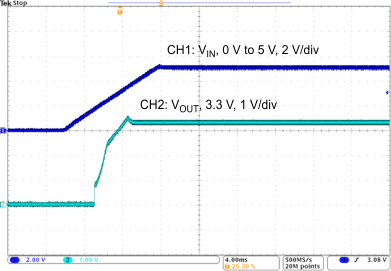
 Figure 24. Power-Up Waveform of TPS76833-Q1