SGLS155B February 2003 – November 2016 TPS768-Q1
PRODUCTION DATA.
- 1 Features
- 2 Applications
- 3 Description
- 4 Revision History
- 5 Pin Configuration and Functions
- 6 Specifications
- 7 Parameter Measurement Information
- 8 Detailed Description
- 9 Application and Implementation
- 10Power Supply Recommendations
- 11Layout
- 12Device and Documentation Support
- 13Mechanical, Packaging, and Orderable Information
8 Detailed Description
8.1 Overview
The TPS768xx-Q1 family includes four fixed-output voltage regulators (1.8 V, 2.5 V, 3.3 V, and 5 V), and offers an adjustable version, the TPS76801-Q1 (adjustable from 1.2 V to 5.5 V).
8.1.1 Device Operation
The TPS768xx-Q1 device features very low quiescent current, which remains virtually constant even with varying loads. Conventional LDO regulators use a PNP pass element, the base current of which is directly proportional to the load current through the regulator (IB = IC / β). The TPS768xx-Q1 device uses a PMOS transistor to pass current. Because the gate of the PMOS is voltage-driven, operating current is low and invariable over the full load range.
Another pitfall associated with the PNP pass element is its tendency to saturate when the device goes into dropout. The resulting drop in β forces an increase in IB to maintain the load. During power up, this translates to large start-up currents. Systems with limited supply current may fail to start up. In battery-powered systems, it means rapid battery discharge when the voltage decays below the minimum required for regulation. The TPS768xx-Q1 quiescent current remains low even when the regulator drops out, eliminating both problems.
The TPS768xx-Q1 family also features a shutdown mode that places the output in the high-impedance state (essentially equal to the feedback-divider resistance) and reduces quiescent current to 2 μA. If the shutdown feature is not used, EN should be tied to ground.
8.2 Functional Block Diagrams
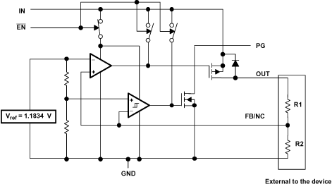
 Figure 20. Functional Block Diagram—Adjustable Version
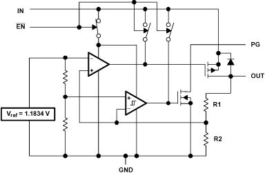
 Figure 21. Functional Block Diagram—Fixed-Voltage Versions
8.3 Feature Description
8.3.1 Power-Good Indicator
The TPS768xx-Q1 device features a power-good (PG) output that can be used to monitor the status of the regulator. The internal comparator monitors the output voltage: when the output drops to between 92% and 98% of its nominal regulated value, the PG output transistor turns on, taking the signal low. The open-drain output requires a pullup resistor. If not used, the PG pin can be left floating. PG can be used to drive power-on reset circuitry or used as a low-battery indicator. PG does not assert itself when the regulated output voltage falls out of the specified 2% tolerance, but instead reports an output voltage low, relative to its nominal regulated value.
8.3.2 Regulator Protection
The TPS768xx-Q1 PMOS-pass transistor has a built-in back diode that conducts reverse currents when the input voltage drops below the output voltage (for example, during power-down). Current is conducted from the output to the input and is not internally limited. When extended reverse voltage is anticipated, external limiting may be appropriate.
The TPS768xx-Q1 device also features internal current limiting and thermal protection. During normal operation, the TPS768xx-Q1 device limits output current to approximately 1.7 A. When current limiting engages, the output voltage scales back linearly until the overcurrent condition ends. While current limiting is designed to prevent gross device failure, care should be taken not to exceed the power dissipation ratings of the package. If the temperature of the device exceeds 150°C (typ), thermal-protection circuitry shuts it down. Once the device has cooled below 130°C (typ), regulator operation resumes.
8.4 Device Functional Modes
8.4.1 Shutdown
The enable pin (EN) is active-low. The device is enabled when the voltage at the EN pin goes below 0.9 V. The device is turned off when the EN pin is held above 1.7 V. When shutdown capability is not required, EN can be connected directly to GND.
8.4.2 Operation With VIN Less Than 2.7 V
The TPS768xx-Q1 family of devices operates with input voltages above 2.7 V. When input voltage falls below 2.7 V, the device shuts down.
8.4.3 Operation With VIN Greater Than 2.7 V
When VIN is greater than 2.7 V, if the input voltage is higher than the desired output voltage plus dropout voltage, the output voltage is equal to the desired value. Otherwise, output voltage will be VIN minus the dropout voltage.