SGLS155B February 2003 – November 2016 TPS768-Q1
PRODUCTION DATA.
- 1 Features
- 2 Applications
- 3 Description
- 4 Revision History
- 5 Pin Configuration and Functions
- 6 Specifications
- 7 Parameter Measurement Information
- 8 Detailed Description
- 9 Application and Implementation
- 10Power Supply Recommendations
- 11Layout
- 12Device and Documentation Support
- 13Mechanical, Packaging, and Orderable Information
11 Layout
11.1 Layout Guidelines
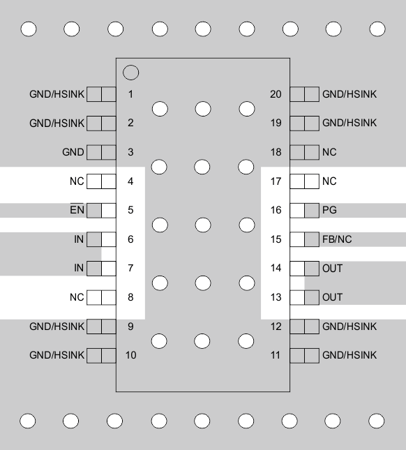
Input and output capacitors should be placed as close to the device pins as possible. To improve ac performance such as PSRR, output noise, and transient response, it is recommended that the board be designed with separate ground planes for IN and OUT, with the ground planes connected only at the GND pin of the device. In addition, the ground connection for the output capacitor should be connected directly to the GND pin of the device. High-ESR capacitors may degrade PSRR performance.
11.2 Layout Example
 Figure 25. TPS768xx-Q1 Layout Example
11.3 Power Dissipation and Junction Temperature
Specified regulator operation is assured to a junction temperature of 125°C; the maximum junction temperature should be restricted to 125°C under normal operating conditions. This restriction limits the power dissipation the regulator can handle in any given application. To ensure the junction temperature is within acceptable limits, calculate the maximum allowable dissipation, PDmax, and the actual dissipation, PD, which must be less than or equal to PDmax.
The maximum power dissipation limit is determined using Equation 3:

where:
TJmax = maximum allowable junction temperature
RθJA = junction-to-ambient thermal resistance for the package; that is, 32.6°C/W for the 20-pin TSSOP (PWP) with no airflow
TA = ambient temperature
The regulator dissipation is calculated using Equation 4:

Power dissipation resulting from quiescent current is negligible. Excessive power dissipation triggers the thermal protection circuit.