SGLS155B February 2003 – November 2016 TPS768-Q1
PRODUCTION DATA.
- 1 Features
- 2 Applications
- 3 Description
- 4 Revision History
- 5 Pin Configuration and Functions
- 6 Specifications
- 7 Parameter Measurement Information
- 8 Detailed Description
- 9 Application and Implementation
- 10Power Supply Recommendations
- 11Layout
- 12Device and Documentation Support
- 13Mechanical, Packaging, and Orderable Information
6 Specifications
6.1 Absolute Maximum Ratings(1)
over operating ambient temperature range (unless otherwise noted)| MIN | MAX | UNIT | |
|---|---|---|---|
| Input voltage, VI (2) | –0.3 | 13.5 | V |
| Voltage at EN | –0.3 | VI + 0.3 | V |
| Maximum PG voltage | 16.5 | V | |
| Peak output current | Internally limited | ||
| Output voltage, VO (OUT, FB) | 7 | V | |
| Operating junction temperature, TJ | –40 | 150 | °C |
| Storage temperature, Tstg | –65 | 150 | °C |
(1) Stresses beyond those listed under Absolute Maximum Ratings may cause permanent damage to the device. These are stress ratings only, and do not imply functional operation of the device at these or any other conditions beyond those indicated under Recommended Operating Conditions. Exposure to absolute-maximum-rated conditions for extended periods may affect device reliability.
(2) All voltage values are with respect to network terminal ground.
6.2 ESD Ratings
| VALUE | UNIT | ||||
|---|---|---|---|---|---|
| V(ESD) | Electrostatic discharge | Human-body model (HBM), per AEC Q100-002(1) | ±2000 | V | |
| Charged-device model (CDM), per AEC Q100-011 | All pins | ±500 | |||
| Corner pins (1, 4, 5, and 8) | ±750 | ||||
(1) AEC Q100-002 indicates that HBM stressing shall be in accordance with the ANSI/ESDA/JEDEC JS-001 specification.
6.3 Recommended Operating Conditions
| MIN | MAX | UNIT | ||
|---|---|---|---|---|
| VI | Input voltage(1) | 2.7 | 10 | V |
| VO | Voltage at OUT | 1.2 | 5.5 | V |
| IO | Output current(2) | 0 | 1 | A |
| TA | Operating ambient temperature(2) | –40 | 125 | °C |
(1) To calculate the minimum input voltage for the maximum output current, use the following equation: VI(min) = VO(max) + V(DO,max_load), where V(DO,max_load) is the dropout voltage at maximum load.
(2) Continuous current and operating junction temperature are limited by internal protection circuitry, but it is not recommended that the device operate under conditions beyond those specified in this table for extended periods of time.
6.4 Thermal Information
| THERMAL METRIC(1) | TPS768xx-Q1 | UNIT | |
|---|---|---|---|
| PWP (HTSSOP) | |||
| 20 PINS | |||
| RθJA | Junction-to-ambient thermal resistance | 39.5 | °C/W |
| RθJC(top) | Junction-to-case (top) thermal resistance | 25.8 | °C/W |
| RθJB | Junction-to-board thermal resistance | 22.1 | °C/W |
| ψJT | Junction-to-top characterization parameter | 0.8 | °C/W |
| ψJB | Junction-to-board characterization parameter | 21.9 | °C/W |
| RθJC(bot) | Junction-to-case (bottom) thermal resistance | 1.7 | °C/W |
(1) For more information about traditional and new thermal metrics, see the Semiconductor and IC Package Thermal Metrics application report, SPRA953.
6.5 Electrical Characteristics
over recommended operating ambient temperature range, VI = VO(typ) + 1 V, IO = 1 mA, EN = 0 V, CO = 10 μF (unless otherwise noted)| PARAMETER | TEST CONDITIONS | MIN | TYP | MAX | UNIT | |||
|---|---|---|---|---|---|---|---|---|
| Output voltage (10-μA to 1-A load)(1) |
TPS76801-Q1 | 5.5 V ≥ VO ≥ 1.5 V | TJ = 25°C | VO | V | |||
| TJ = –40°C to 125°C | 0.98 × VO | 1.02 × VO | ||||||
| TPS76818-Q1 | 2.8 V < VIN < 10 V | TJ = 25°C | 1.8 | |||||
| TJ = –40°C to 125°C | 1.764 | 1.836 | ||||||
| TPS76825-Q1 | 3.5 V < VIN < 10 V | TJ = 25°C | 2.5 | |||||
| TJ = –40°C to 125°C | 2.45 | 2.55 | ||||||
| TPS76833-Q1 | 4.3 V < VIN < 10 V | TJ = 25°C | 3.3 | |||||
| TJ = –40°C to 125°C | 3.234 | 3.366 | ||||||
| TPS76850-Q1 | 6 V < VIN < 10 V | TJ = 25°C | 5 | |||||
| TJ = –40°C to 125°C | 4.9 | 5.1 | ||||||
| Quiescent current (GND current), EN = 0 V(1) | TJ = 25°C 10 μA < IO < 1 A, TJ = 25°C | 85 | μA | |||||
| TJ = –40°C to 125°C IO = 1 A, TJ = –40°C to 125°C | 125 | |||||||
| Output voltage line regulation (ΔVO / VO) (1) (2) | TJ = 25°C VO + 1 V < VI ≤ 10 V, TJ = 25°C | 0.01 | %/V | |||||
| Load regulation | 3 | mV | ||||||
| Output noise voltage | TPS76818-Q1 | TJ = 25°C BW = 200 Hz to 100 kHz, CO = 10 μF, IC = 1 A, TJ = 25°C | 55 | μVrms | ||||
| Output current limit | VO = 0 V | 1.7 | 2 | A | ||||
| Thermal shutdown junction temperature | 150 | °C | ||||||
| Standby current | EN = VI, 2.7 V < VI < 10 V |
TJ = 25°C | 1 | μA | ||||
| TJ = –40°C to 125°C | 10 | |||||||
| FB input current | TPS76801-Q1 | VFB = 1.5 V | 2 | nA | ||||
| High-level enable input voltage | 1.7 | V | ||||||
| Low-level enable input voltage | 0.9 | V | ||||||
| Power-supply ripple rejection (1) | TJ = 25°C f = 1 kHz, CO = 10 μF, TJ = 25°C | 60 | dB | |||||
| PG | Minimum input voltage for valid PG | IO(PG) = 300 μA | 1.1 | V | ||||
| Trip threshold voltage | VO decreasing | 92 | 98 | %VO | ||||
| Hysteresis voltage | Measured at VO | 0.5 | %VO | |||||
| Output low voltage | VI = 2.7 V, IO(PG) = 1 mA | 0.15 | 0.4 | V | ||||
| Leakage current | V(PG) = 5 V | 1 | μA | |||||
| EN input current | EN = 0 V | –1 | 0 | 1 | μA | |||
| EN = VI | –1 | 1 | ||||||
| Dropout voltage (3) | TPS76833-Q1 | IO = 1 A | TJ = 25°C | 350 | mV | |||
| TJ = –40°C to 125°C | 575 | |||||||
| TPS76850-Q1 | TJ = 25°C | 230 | ||||||
| TJ = –40°C to 125°C | 380 | |||||||
(1) Minimum IN operating voltage is 2.7 V or VO(typ) + 1 V, whichever is greater. Maximum IN voltage 10 V.
(2) If VO ≤ 1.8 V then VI(max) = 10 V, VI(min) = 2.7 V: 
If VO ≥ 2.5 V then VI(max) = 10 V, VI(min) = VO + 1 V:

If VO ≥ 2.5 V then VI(max) = 10 V, VI(min) = VO + 1 V:

(3) IN voltage equals VO(typ) – 100 mV.
6.6 Typical Characteristics
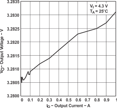 Figure 1. TPS76833-Q1 Output Voltage vs Output Current
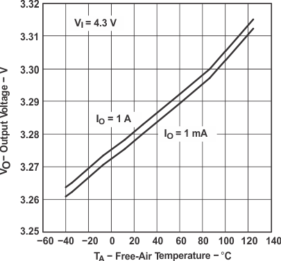 Figure 3. TPS76833-Q1 Output Voltage vs Ambient Temperature
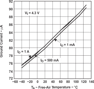 Figure 5. TPS76833-Q1 Ground Current vs Ambient Temperature
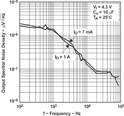 Figure 7. TPS76833-Q1 Output Spectral Noise Density vs Frequency
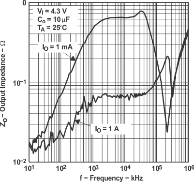 Figure 9. TPS76833-Q1 Output Impedance vs Frequency
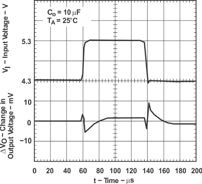 Figure 11. TPS76833-Q1 Line Transient Response
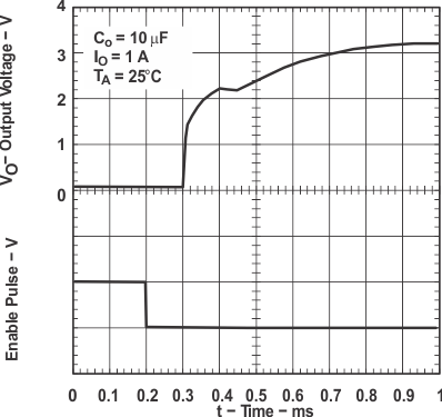 Figure 13. TPS76833-Q1 Output Voltage vs Time (at Start-Up)
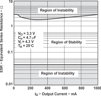 Figure 15. Typical Region of Stability Equivalent Series Resistance Equivalent series resistance (ESR) refers to the total series resistance, including the ESR of the capacitor, any series resistance added externally, and PWB trace resistance to C vs Output Current
1. Equivalent series resistance (ESR) refers to the total series resistance, including the ESR of the capacitor, any series resistance added externally, and PWB trace resistance to CO.
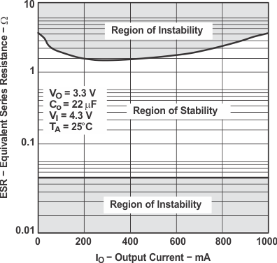 Figure 17. Typical Region of Stability Equivalent Series Resistance(1) vs Output Current
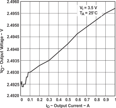 Figure 2. TPS76825-Q1 Output Voltage vs Output Current
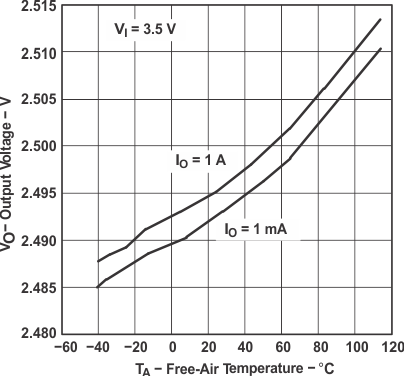 Figure 4. TPS76825-Q1 Output Voltage vs Ambient Temperature
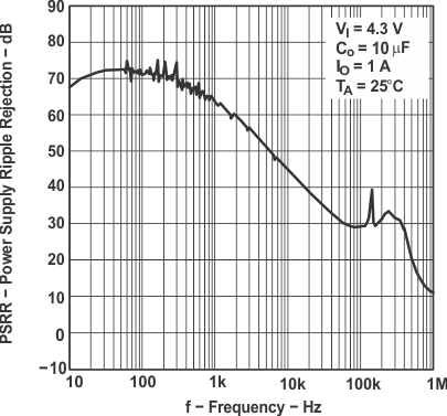 Figure 6. TPS76833-Q1 Power-Supply Ripple Rejection vs Frequency
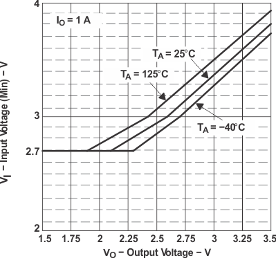 Figure 8. Input Voltage (Min.) vs Output Voltage
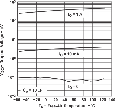 Figure 10. TPS76833-Q1 Dropout Voltage vs Ambient Temperature
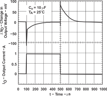 Figure 12. TPS76833-Q1 Load Transient Response
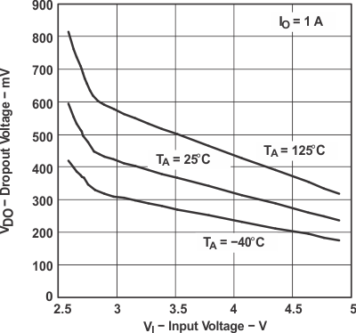 Figure 14. TPS76801-Q1 Dropout Voltage vs Input Voltage
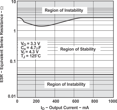 Figure 16. Typical Region of Stability Equivalent Series Resistance(1) vs Output Current
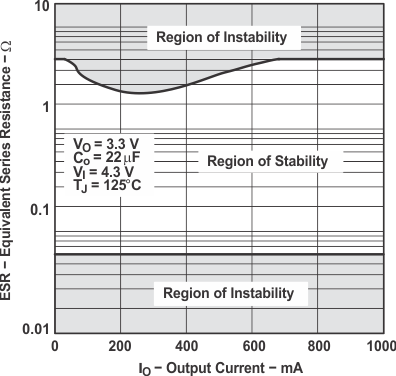 Figure 18. Typical Region of Stability Equivalent Series Resistance(1) vs Output Current