ZHCSN73B January 2021 – January 2022 TPS785-Q1
PRODUCTION DATA
- 1 特性
- 2 应用
- 3 说明
- 4 Revision History
- 5 Pin Configuration and Functions
- 6 Specifications
- 7 Detailed Description
-
8 Application and Implementation
- 8.1 Application Information
- 8.2 Typical Application
- 9 Power Supply Recommendations
- 10Layout
- 11Device and Documentation Support
- 12Mechanical, Packaging, and Orderable Information
封装选项
机械数据 (封装 | 引脚)
散热焊盘机械数据 (封装 | 引脚)
订购信息
8.1.9.2 Recommended Area for Continuous Operation
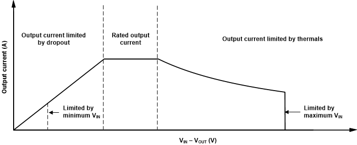
The operational area of an LDO is limited by the dropout voltage, output current, junction temperature, and input voltage. The recommended area for continuous operation for a linear regulator is given in Figure 8-6 and can be separated into the following parts:
- Dropout voltage limits the minimum differential voltage between the input and the output (VIN – VOUT) at a given output current level. See the Section 8.1.6 section for more details.
- The rated output currents limits the maximum recommended output current level. Exceeding this rating causes the device to fall out of specification.
- The rated junction temperature limits the maximum junction temperature of the device. Exceeding this rating causes the device to fall out of specification and reduces long-term reliability.
- The shape of the slope is given by Equation 6. The slope is nonlinear because the maximum rated junction temperature of the LDO is controlled by the power dissipation across the LDO; thus when VIN – VOUT increases the output current must decrease.
- The rated input voltage range governs both the minimum and maximum of VIN – VOUT.
Figure 8-6 shows the recommended area of operation for this device on a JEDEC-standard high-K board with a RθJA as given in the Recommended Operating Conditions table.
 Figure 8-6 Region Description of Continuous Operation Regime