SLVS389M September 2002 – September 2015 TPS786
PRODUCTION DATA.
- 1 Features
- 2 Applications
- 3 Description
- 4 Revision History
- 5 Pin Configuration and Functions
- 6 Specifications
- 7 Detailed Description
- 8 Application and Implementation
- 9 Power Supply Recommendations
- 10Layout
- 11Device and Documentation Support
- 12Mechanical, Packaging, and Orderable Information
封装选项
机械数据 (封装 | 引脚)
散热焊盘机械数据 (封装 | 引脚)
订购信息
5 Pin Configuration and Functions
DCQ Package
6-Pin SOT-223
Top View

DRB Package
8-SON
Top View

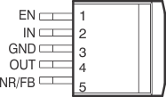
KTT Package
5-Pin TO-263
Top View

Pin Functions
| PIN | I/O | DESCRIPTION | |||
|---|---|---|---|---|---|
| NAME | SOT-223 | TO-263 | SON | ||
| NR | 5 | 5 | 5 | — | Noise-reduction pin for fixed versions only. An external bypass capacitor, connected to this terminal, in conjunction with an internal resistor, creates a low-pass filter to further reduce regulator noise. |
| EN | 1 | 1 | 8 | I | The EN terminal is an input that enables or shuts down the device. When EN is a logic high, the device is enabled. When the device is a logic low, the device is in shutdown mode. |
| FB | 5 | 5 | 5 | I | Feedback input voltage for the adjustable device. |
| GND | 3, 6 | 3, TAB | 6 | — | Regulator ground |
| IN | 2 | 2 | 1, 2 | I | Input supply |
| OUT | 4 | 4 | 3, 4 | O | Regulator output |