SGLS162I April 2003 – March 2016 TPS793-Q1
PRODUCTION DATA.
- 1 Features
- 2 Applications
- 3 Description
- 4 Revision History
- 5 Voltage Options
- 6 Pin Configuration and Functions
- 7 Specifications
- 8 Detailed Description
- 9 Application and Implementation
- 10Power Supply Recommendations
- 11Layout
- 12Device and Documentation Support
- 13Mechanical, Packaging, and Orderable Information
11 Layout
11.1 Layout Guidelines
Layout is a critical part of good power-supply design. There are several signal paths that conduct fast-changing currents or voltages that can interact with stray inductance or parasitic capacitance to generate noise or degrade the power-supply performance. To help eliminate these problems, the IN pin should be bypassed to ground with a low ESR ceramic bypass capacitor with an X5R or X7R dielectric.
Equivalent series inductance (ESL) and equivalent series resistance (ESR) must be minimized to maximize performance and ensure stability. Every capacitor (CIN, COUT, CNR/SS, CFF) must be placed as close as possible to the device and on the same side of the PCB as the regulator itself. Do not place any of the capacitors on the opposite side of the PCB from where the regulator is installed. The use of vias and long traces is strongly discouraged because these circuits may impact system performance negatively, and even cause instability
11.1.1 Board Layout Recommendations to Improve PSRR and Noise Performance
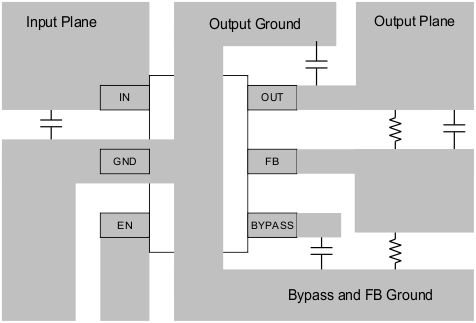
To improve AC measurements like PSRR, output noise, and transient response, it is recommended that the board be designed with separate ground planes for VIN and VOUT, with each ground plane connected only at the GND pin of the device. In addition, the ground connection for the bypass capacitor should connect directly to the GND pin of the device.
11.2 Layout Example
 Figure 28. Layout Example (DBV Package)
11.3 Power Dissipation and Junction Temperature
Specified regulator operation is ensured to a junction temperature of 125°C; the maximum junction temperature should be restricted to 125°C under normal operating conditions. This restriction limits the power dissipation the regulator can handle in any given application. To ensure the junction temperature is within acceptable limits, calculate the maximum allowable dissipation, PD(max), and the actual dissipation, PD, which must be less than or equal to PD(max).
The maximum power dissipation limit is determined using Equation 4.

where
- TJmax = Maximum allowable junction temperature
- RθJA = Thermal resistance, junction to ambient, for the package, see the Thermal Information table
- TA = Ambient temperature
The regulator dissipation is calculated using Equation 5.

Power dissipation resulting from quiescent current is negligible. Excessive power dissipation triggers the thermal protection circuit.